Photocuring device

Pending Publication Date: 2021-05-20
COSMEX
View PDF0 Cites 0 Cited by
  • Summary
  • Abstract
  • Description
  • Claims
  • Application Information

AI Technical Summary

Benefits of technology

The present invention is a photocuring device that has low material and production costs. It allows for the display and operation interface to be placed at any position on the device, without constraints on size, shape, or angle. Additionally, the device allows for the display and operation interface to be simplified for easy operation and viewing by a manicurist or person receiving a manicure.

Problems solved by technology

Heat curing has the disadvantages of slow speed, poor energy efficiency, and long time required; in addition, it will produce bad odors due to solvent volatilization during operation, and may also deform the patterns on the nail surface due to the application of hot air.
The foregoing configurations, however, make it difficult to elevate the exterior of those devices esthetically.
If the operation interface and the display interface are to be integrated into a touch panel, the cost of the resulting devices will be increased significantly.
Moreover, a touch panel as well as a display screen must match in shape and size the location where it is mounted, but it is difficult to make a touch panel or display screen of an irregular or exceptionally large or small shape.
A touch panel or display screen must also be planar and therefore tends to have problem adapting to locations with a large curvature.
Consequently, a photocuring device not only is subject to design limitations imposed on its shape and size, but also is complicated in terms of manufacture.

Method used


Image

  • Photocuring device
  • Photocuring device
  • Photocuring device

Examples


embodiment 1

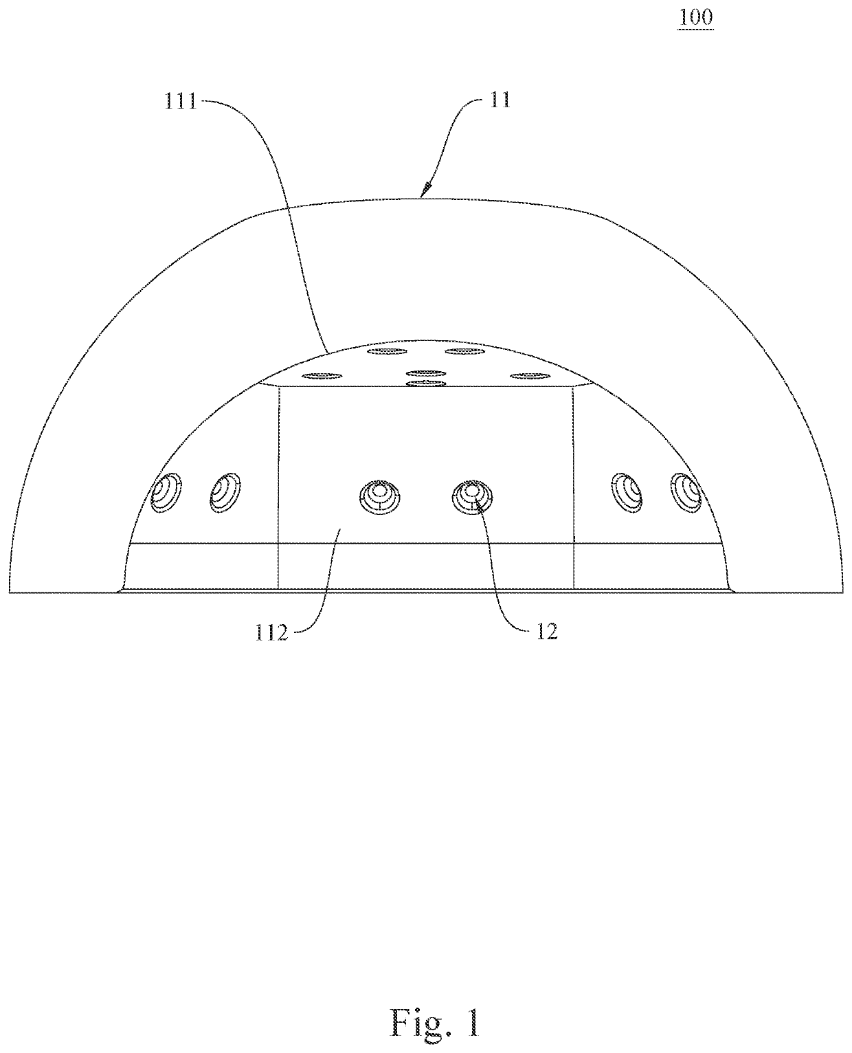
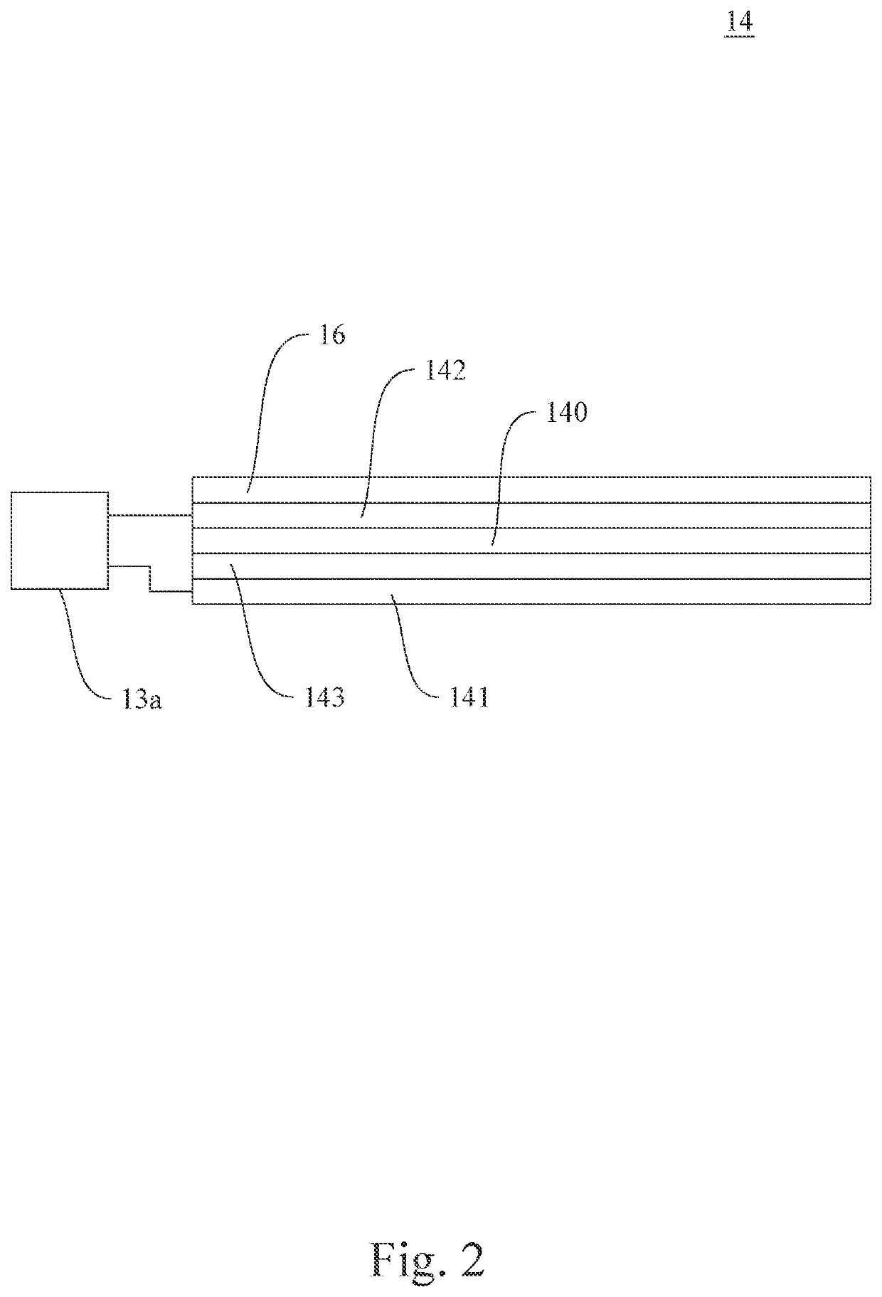
[0035]Please refer to FIG. 1 and FIG. 2 respectively for a perspective view of the photocuring device 100 according to a preferred embodiment of the present invention and a schematic drawing of the electrical means adopted by the photocuring device.

[0036]The photocuring device 100 according to this embodiment includes a housing 11 and an ultraviolet (UV) light module 12. The housing 11 includes an electroluminescent layer 140 and a control module 13a directly or indirectly connected to the electroluminescent layer 140 by an electrical means. The housing 11 may also include a protective layer 16 as its outermost layer. The housing 11 may also comprise at least one LED light (not shown) providing different color lights, which decorates the photocuring device 100.

[0037]One side of the housing 11 is formed at least with a cavity 112 with an opening 111. The housing 11 serves to support and secure the entire structure of the photocuring device 100 and prevent the light emitted by UV ligh...

embodiment 2

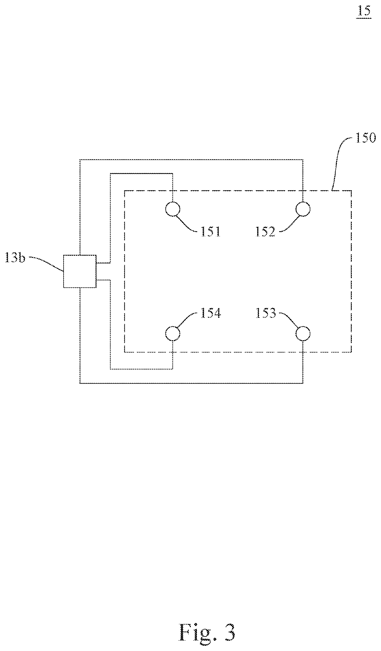
[0049]Please refer to FIG. 1 and FIG. 3 respectively for a perspective view of the photocuring device 100 according to another preferred embodiment of the present invention and a schematic drawing of the electrical means adopted by this photocuring device.

[0050]The photocuring device 100 according to this embodiment includes a housing 11 and a UV light module 12, both of which are identical to their counterparts in embodiment 1. Embodiment 2 further includes a touch layer 150 and a control module 13b connected to the touch layer 150 by an electrical means, wherein the touch layer 150 is included in the housing 11. The control module 13b includes a control circuit board for controlling the UV light module 12. Embodiment 2 may also include a protective layer (not shown) as needed.

[0051]The touch layer 150 in the present invention involves electric sensing and achieves interaction in a free space. For example, when a user's body part enters the sensing area, the electric current distri...

embodiment 3

[0057]Please refer to FIG. 1, FIG. 4, and FIG. 5 respectively for a perspective view of the photocuring device 100 according to yet another preferred embodiment of the present invention, a schematic drawing of the electrical means adopted by this photocuring device, and schematic drawings showing possible locations of the electroluminescent module 14 and / or the touch control module 15.

[0058]The photocuring device 100 according to this embodiment includes a housing 11 and a UV light module 12, both of which are identical to their counterparts in embodiment 1. Embodiment 3 is different from the previous embodiments in that the photocuring device, or more particularly the housing 11, includes both the electroluminescent module 14 and the touch control module 15. The control module 13c in this embodiment is electrically connected to the electroluminescent module 14 and the touch control module 15 by an electrical means. If necessary, embodiment 3 may also include a plurality of protecti...


PUM

PropertyMeasurementUnit
Timeaaaaaaaaaa
Sizeaaaaaaaaaa
Shapeaaaaaaaaaa

Abstract

The present invention provides a photocuring device, comprising a housing and an ultraviolet (UV) light module, wherein the housing comprises an electroluminescent layer and / or a touch layer and a control module connected to the electroluminescent layer and / or the touch layer by an electrical means. The photocuring device of the invention not only features a low material cost and low production cost, but also allows its display interface and / or operation interface to be provided at any position of the housing of the photocuring device, without limitations in size, shape, or angle. Furthermore, the photocuring device of the invention allows its display interface and / or operation interface to be simplified as needed to facilitate operation and viewing by a manicurist or one who is receiving a manicure.

Description

BACKGROUND OF THE INVENTION1. Technical Field[0001]The present invention relates to a photocuring device and more particularly to a photocuring device with a simplified display interface and / or operation interface.2. Description of Related Art[0002]Nail art has become popular in many countries in recent years. Generally, the curing methods of nail art can be divided into heat curing and photocuring. Heat curing has the disadvantages of slow speed, poor energy efficiency, and long time required; in addition, it will produce bad odors due to solvent volatilization during operation, and may also deform the patterns on the nail surface due to the application of hot air. Therefore, in recent years, the curing method of nail art has been photocuring as the mainstream.[0003]In the process of photocuring the glue applied on the nails, the photocuring device (or machine) must be operated to control the light irradiation process and time to achieve the ideal photocuring effect. Therefore, the...

Claims


Application Information

Patent Timeline
IPC IPC(8): B01J19/12A45D29/00B29C35/08
CPCB01J19/123B01J2219/1203B29C35/08A45D29/00
Inventor HSIEH, WAN-CHIEHWU, YA-WENLI, YU-CHINGCHUNG, WEN-SHAN
Owner COSMEX
Why Eureka
Try Eureka