

Image display element and method for manufacturing image display element
a technology of image display element and manufacturing method, which is applied in the direction of identification means, instruments, semiconductor devices, etc., can solve the problems of reducing the internal quantum efficiency of the led, unable to achieve the expected light emission efficiency, and the led needs to be smaller, so as to improve the light emission efficiency of the micro light emitting element, improve the effect of light emission efficiency and high efficiency
- Summary
- Abstract
- Description
- Claims
- Application Information
AI Technical Summary
Benefits of technology
Problems solved by technology
Method used
Image

Examples
first embodiment
Configuration of Image Display Element 200
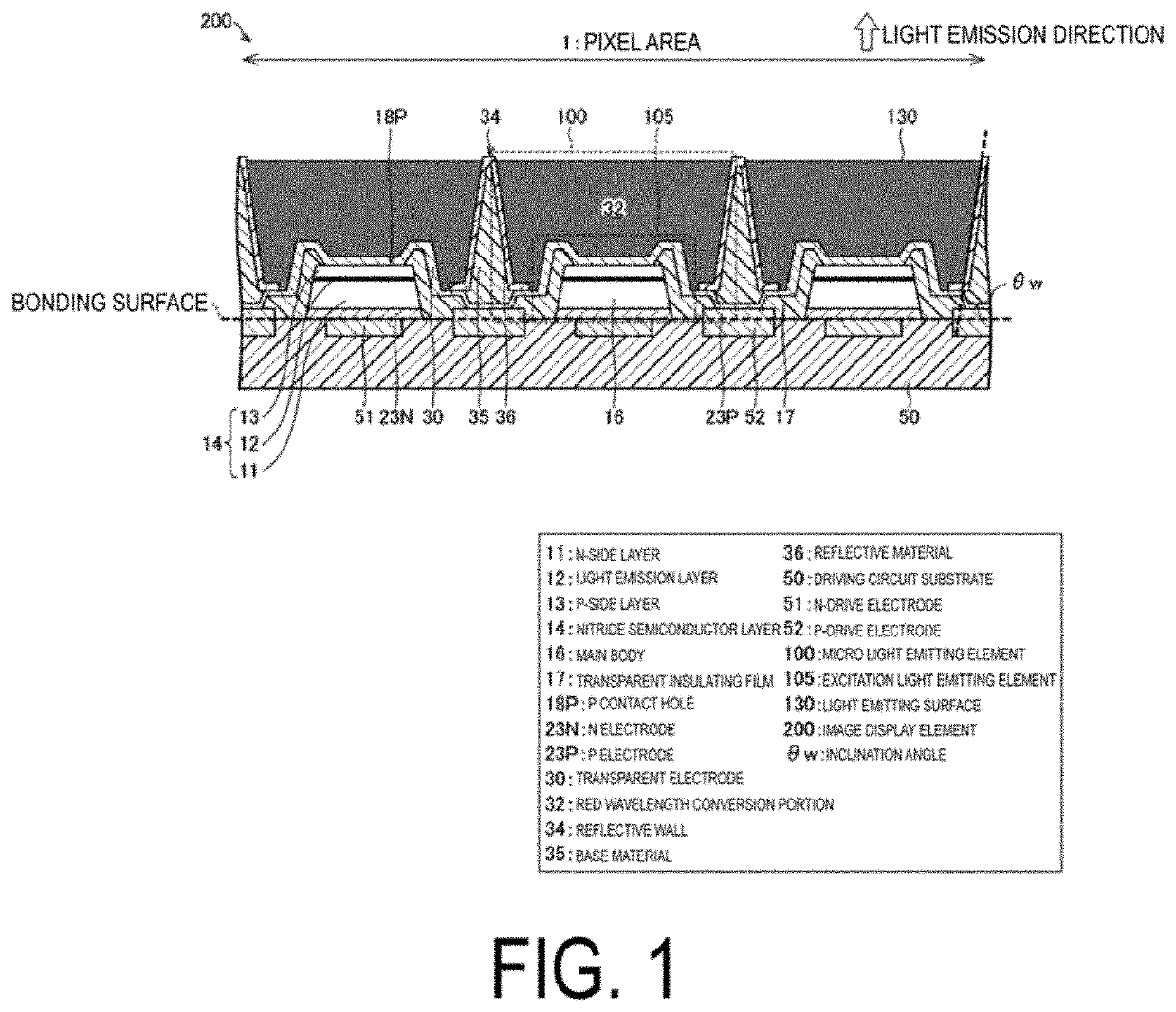
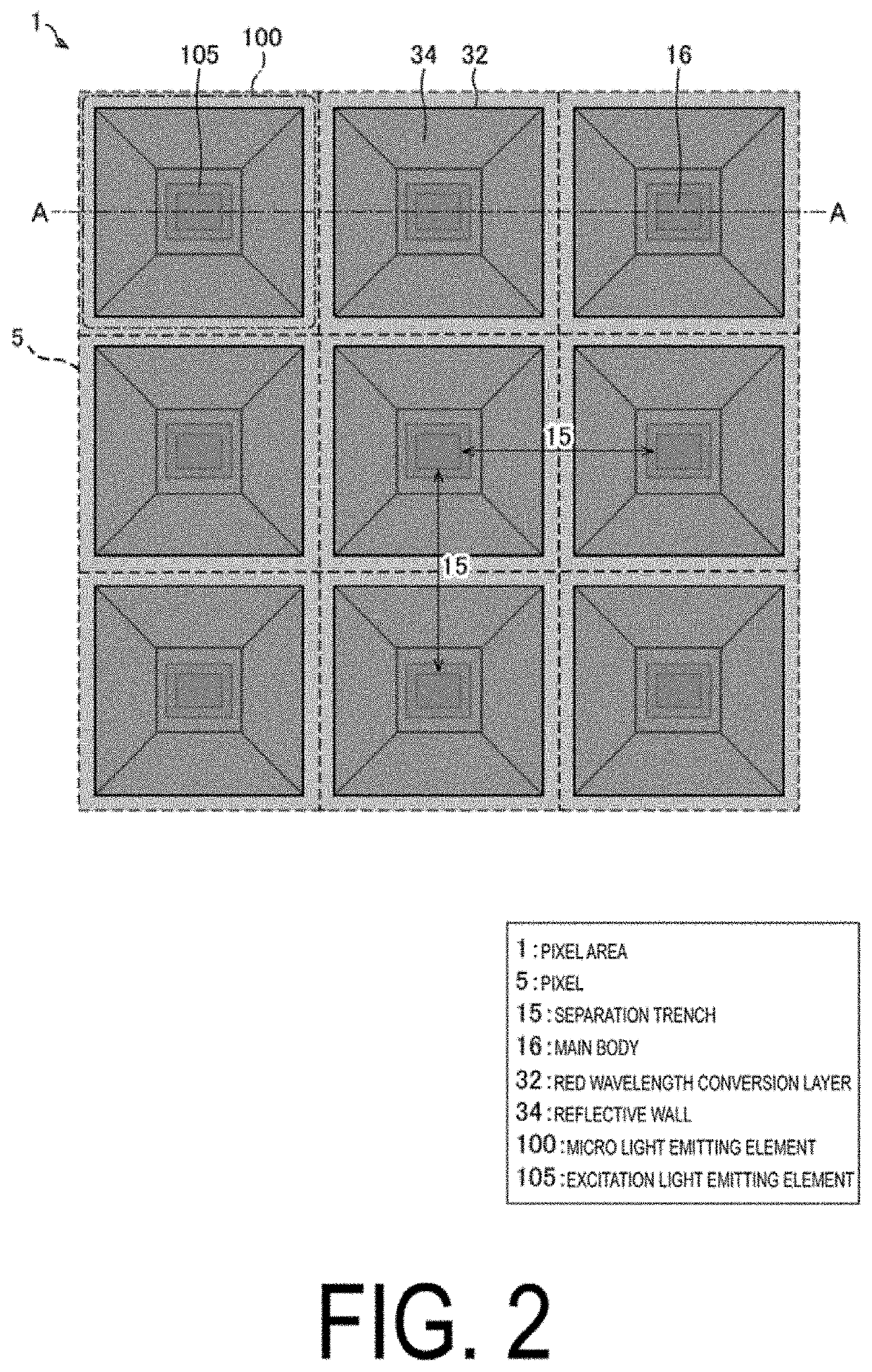
[0071]FIG. 1 is a cross-sectional schematic view of a pixel area 1 of an image display element 200 according to a first embodiment of the disclosure. FIG. 2 is a schematic plan view of the pixel area 1 of the image display element 200 according to the first embodiment of the disclosure. FIG. 1 illustrates a cross-sectional view at the portion of the A-A line of FIG. 2. As illustrated in FIG. 2, an upper surface of the image display element 200 is a pixel area 1 in which a plurality of pixels 5 are disposed in an array. In the present embodiment, the image display element 200 is a single color display element, and each of the pixels 5 includes a single color micro light emitting element 100. As illustrated in FIG. 2, in the pixel area 1, the pixels 5 are disposed in an array, each pixel 5 emits red light, and a red single color image is displayed by adjusting the intensity of each of the pixels 5.
[0072]The micro light emitting element 100 inc...
second embodiment
Configuration of Image Display Element 200a
[0110]Another embodiment of the disclosure will be described below with reference to FIGS. 5 and 6. Note that, for convenience of description, components having the same functions as those described in the embodiment described above will be denoted by the same reference signs, and descriptions of those components will be omitted. The image display element 200a of the second embodiment has a configuration similar to that of the first embodiment; however, differs in that the display element is a full color display element rather than a single color display element.
[0111]As illustrated in FIG. 5, the image display element 200a includes a plurality of blue micro light emitting elements 100B, a plurality of red micro light emitting elements 100R, a plurality of green micro light emitting elements 100G, and a driving circuit substrate 50. The driving circuit substrate 50 supplies current to the blue micro light emitting element 100B, the red mic...
third embodiment
[0118]Configuration of Image Display Element 200b
[0119]Another embodiment of the disclosure will be described below with reference to FIGS. 8 to 9C. Note that, for convenience of description, components having the same functions as those described in the embodiments described above will be denoted by the same reference signs, and descriptions of those components will be omitted. The image display element 200b according to the third embodiment differs from the second embodiment in that the P-drive electrode 52 is not disposed in the pixel area 1. Other points are the same as in the second embodiment.
[0120]As illustrated in FIG. 8, a plurality of blue micro light emitting elements 100Bb, a plurality of red micro light emitting elements 100Rb, and a plurality of green micro light emitting elements 100Gb constituting the image display element 200b each have only the N electrode 23N in the pixel area 1, and the transparent electrode 30 connected to the P-side layer 13 is connected to th...
PUM
 Abstract
Description
Claims
Application Information