Power distribution/coupling circuit and power distribution/coupling component
- Summary
- Abstract
- Description
- Claims
- Application Information
AI Technical Summary
Benefits of technology
Problems solved by technology
Method used
Image
Examples
first preferred embodiment
Power Distribution / Coupling Circuit 100
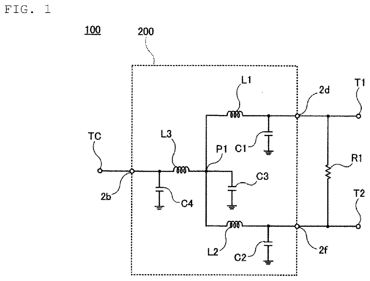
[0034]FIG. 1 shows an equivalent circuit diagram of a power distribution / coupling circuit 100 according to a first preferred embodiment of the present invention. In FIG. 1, a portion of the circuit is surrounded by a broken line, and as will be described later, this portion is defined by a power distribution / coupling component 200 in the present preferred embodiment.
[0035]The power distribution / coupling circuit 100 includes a common terminal TC, a first terminal T1, and a second terminal T2. Further, the power distribution / coupling circuit 100 includes a first connection point P1.
[0036]A first inductor L1 is connected between the first connection point P1 and the first terminal T1. Further, a second inductor L2 is connected between the first connection point P1 and the second terminal T2.
[0037]A first capacitor C1 is shunt-connected between an end of the first inductor L1 closer to the first terminal T1 and a ground. Further, a second capacitor...
example 1
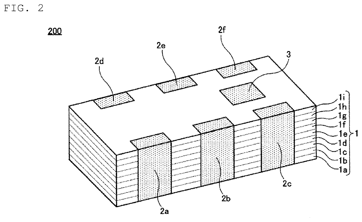
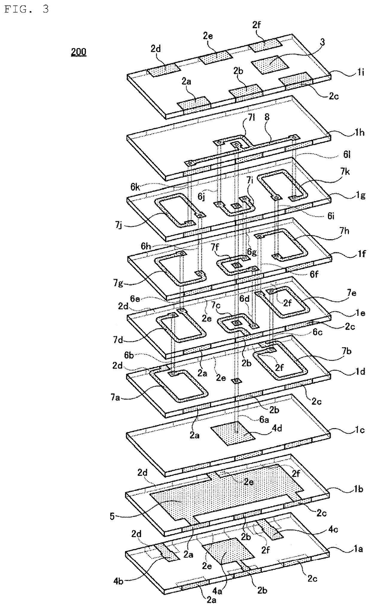
[0077]In Example 1, the power distribution / coupling component 200 having the structure shown in FIGS. 2, 3, and 4 was manufactured, and the power distribution / coupling component 200 and the resistor R1 were used to manufacture the power distribution / coupling circuit 100 shown in FIG. 1. Table 1 shows an inductance value of the inductors, a capacitance value of the capacitors, and a resistance value of the resistor. The inductance value of the first inductor L1 and the inductance value of the second inductor L2 are set to the same or substantially the same value, and the capacitance value of the first capacitor C1 and the capacitance value of the second capacitor C2 are set to the same or substantially the same value.
TABLE 1L1C1L2L3C2C3C4R115.5 nH4.0 nH5.3 pF7.0 pF3.5 pF100 Ω
[0078]Further, for comparison, a power distribution / coupling circuit in Comparative Example 1 was manufactured. In the comparative example, the third inductor L3 and the fourth capacitor C4 are removed from Examp...
second preferred embodiment
Power Distribution / Coupling Circuit 300
[0082]FIG. 6 shows an equivalent circuit diagram of a power distribution / coupling circuit 300 according to a second preferred embodiment of the present invention. In FIG. 6, a portion of the circuit is surrounded by a broken line, and as will be described below, this portion is defined by a power distribution / coupling component 400 in the present preferred embodiment.
[0083]The power distribution / coupling circuit 300 according to the second preferred embodiment is configured by modifying a portion of the configuration of the power distribution / coupling circuit 100 according to the first preferred embodiment. Specifically, in the power distribution / coupling circuit 300, the first inductor L1 of the power distribution / coupling circuit 100 is divided into two inductors L1A and L1B at a second connection point P2. Similarly, in the power distribution / coupling circuit 300, the second inductor L2 of the power distribution / coupling circuit 100 is divid...
PUM
 Abstract
Description
Claims
Application Information


