Organic light-emitting diode display panel

a light-emitting diode and display panel technology, applied in the field of displays, can solve the problems of affecting the subsequent production process, the difficulty of separation, and so as to reduce the difficulty of subsequent processing, improve the adhesion stability, and avoid the effect of affecting the display quality of the display panel

Inactive Publication Date: 2021-06-10
WUHAN CHINA STAR OPTOELECTRONICS SEMICON DISPLAY TECH CO LTD
View PDF0 Cites 0 Cited by
  • Summary
  • Abstract
  • Description
  • Claims
  • Application Information

AI Technical Summary

Benefits of technology

[0010]The barrier is disposed on a side of the display panel adjacent to the non-display area. The barrier covers one or more different film layers, and is configured to prevent the anisotropic conductive film from overflowing from an edge of the non-display area.
[0021]In the OLED display panel of the present disclosure, by setting the barrier in the display panel, the barrier covers the plurality of different film layers, and is configured to prevent the anisotropic conductive film from overflowing from the display panel, thereby reducing a difficulty of subsequent processing, and avoiding affecting a display quality of the display panel.
[0022]The barrier includes a groove and a retaining wall structure. Numbers of film layers covered by the groove and the retaining wall structure are the same. That is, the depth of the groove is equal to the thickness of the retaining wall structure. A combination of one or more different film layers including the pixel definition layer can improve an adhesion stability between the display panel and the flexible printed circuit board and effectively prevent the anisotropic conductive film overflowing from the edge of the non-display area, which will affect the display quality of the display panel.

Problems solved by technology

It is difficult to separate them, which affects a subsequent production process and a display quality of the display panel.

Method used


Image

  • Organic light-emitting diode display panel
  • Organic light-emitting diode display panel
  • Organic light-emitting diode display panel

Examples


Embodiment Construction

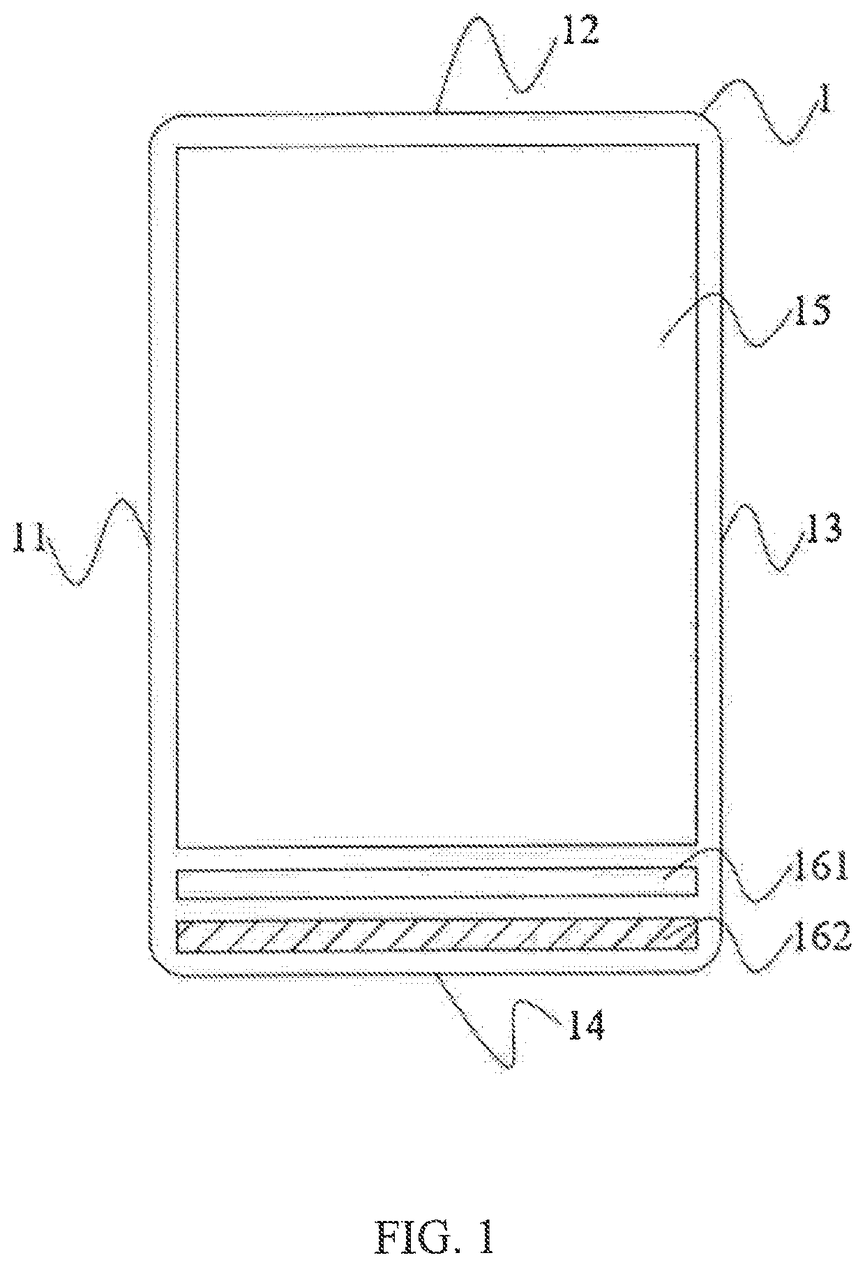
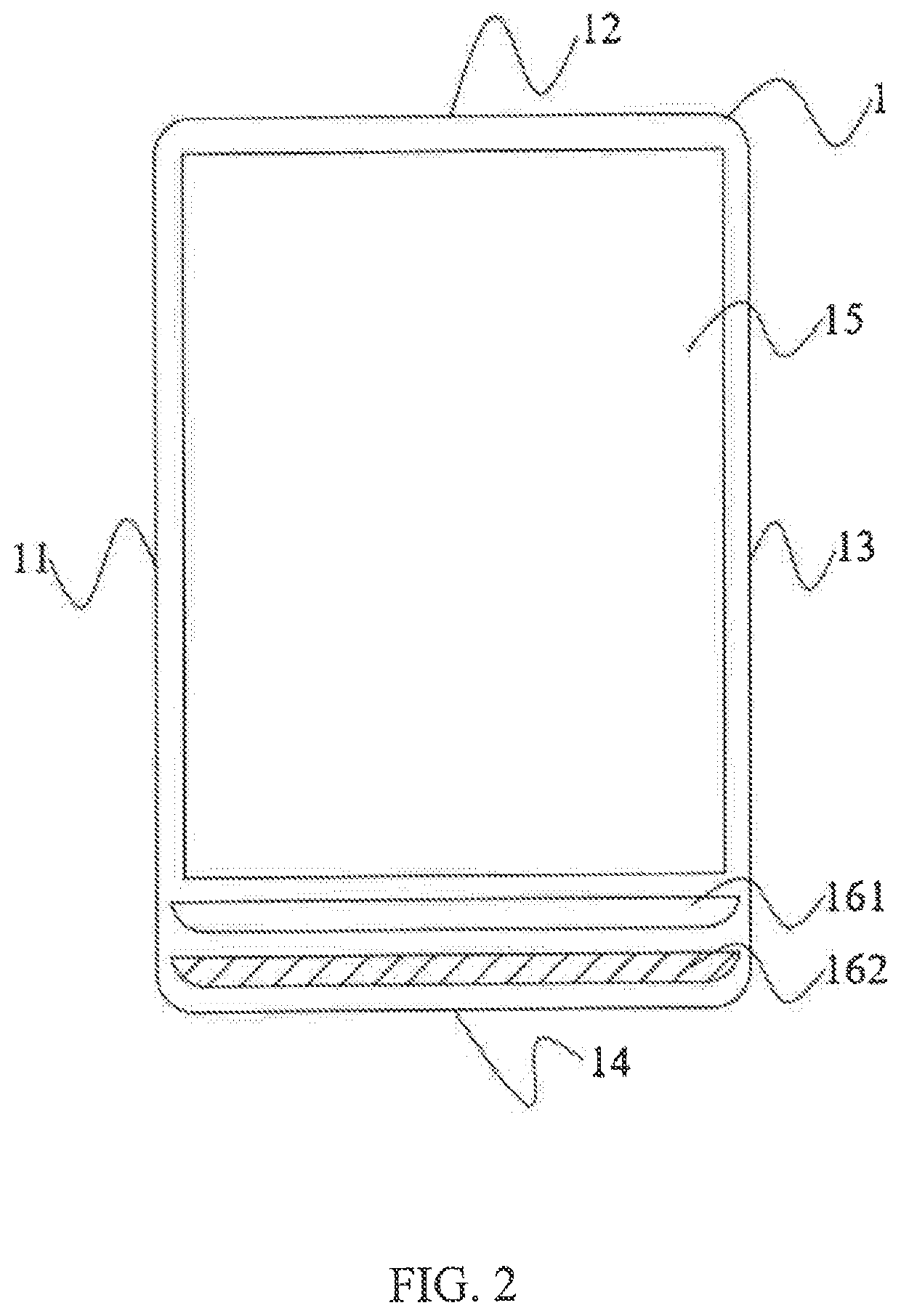
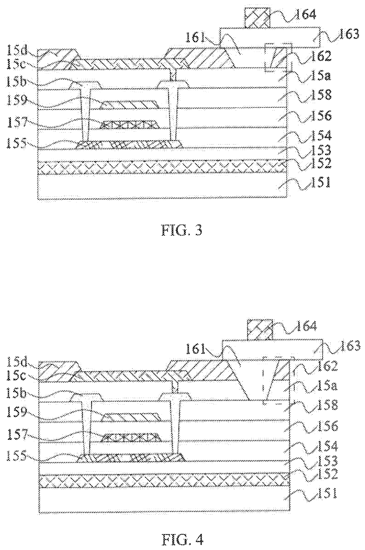
[0034]The following clearly and completely describes the technical solutions in the embodiments of the present disclosure with reference to the accompanying drawings in the embodiments of the present disclosure. Apparently, the described embodiments are merely some but not all of the embodiments of the present disclosure. All other embodiments obtained by a person skilled in the art based on the embodiments of the present disclosure without creative efforts shall fall within the protection scope of the present disclosure.

[0035]In the specification of the present disclosure, it is to be understood that terms such as “central”, “longitudinal”, “lateral”, “length”, “width”, “thickness”, “upper”, “lower”, “front”, “rear”, “left”, “right”, “vertical”, “horizontal”, “top”, “bottom”, “inner”, “outer”, “clockwise”, and “counterclockwise” should be construed to refer to the orientation as then described or as shown in the drawings under discussion. These relative terms are for convenience of...


PUM

PropertyMeasurementUnit
flexibleaaaaaaaaaa
conductiveaaaaaaaaaa
anisotropic conductiveaaaaaaaaaa

Abstract

An organic light-emitting diode display panel, including a display area, a non-display area. A plurality of different film layers are disposed in the display area and the non-display area. A flexible printed circuit board is disposed in the non-display area. An anisotropic conductive film is configured to attach the display panel with the flexible printed circuit board. A barrier is disposed on a side of the display panel adjacent to the non-display area. A barrier covers one or more different film layers, and is configured to prevent the anisotropic conductive film from overflowing from an edge of the non-display area.

Description

CROSS REFERENCE TO RELATED APPLICATIONS[0001]This application claims the priority of a Chinese Patent Application No. 201911238605.3, filed on Dec. 6, 2019, titled “ORGANIC LIGHT EMITTING DIODE DISPLAY PANEL AND DISPLAY DEVICE”, the entire contents of which are incorporated herein by reference.FIELD OF DISCLOSURE[0002]The present disclosure relates to the field of displays, and particularly to organic light-emitting diode (OLED) display panels.BACKGROUND[0003]An existing OLED display panels has a profound impact on applications of wearable devices due to its low power consumption and flexible characteristics. In the future, flexible screens will be widely used with a continuous penetration of personal smart terminals. However, during a production process of the OLED display panel, an anisotropic conductive film (ACF) disposed between a display panel and a flexible printed circuit board on the display panel is melted by heat, and it will overflow from the display panel and flow to an...

Claims


Application Information

Patent Timeline
Patent Type & Authority Applications(United States)
IPC IPC(8): H01L27/32H05K1/18
CPCH01L27/3276H01L27/3246H01L51/0097H05K2201/10128H05K1/189H10K59/123H10K59/124H10K59/126H10K59/1213H10K59/122H05K3/323H10K71/80H10K59/1201H10K2102/311H10K59/131H10K71/00H10K77/111
Inventor ZHOU, SISI
Owner WUHAN CHINA STAR OPTOELECTRONICS SEMICON DISPLAY TECH CO LTD
Why Eureka
Try Eureka