High-frequency switch

a high-frequency switch and switch technology, applied in the field of high-frequency switches, to achieve the effect of suppressing signal leakage through the gate and back gate upon the cut-o

Active Publication Date: 2021-06-10
MITSUBISHI ELECTRIC CORP
View PDF0 Cites 0 Cited by
  • Summary
  • Abstract
  • Description
  • Claims
  • Application Information

AI Technical Summary

Benefits of technology

[0008]The high-frequency switch according to the invention includes the first switching circuit that is disposed in parallel with the resistive element between the back gate and the high-frequency ground, and causes a short circuit between the back gate and the high-frequency ground upon cut-off. By this, signal leakage through the gate and back gate upon the cut-off can be suppressed.

Problems solved by technology

At this time, when the gate or a back gate is biased at a fixed potential, Vgs (source-gate voltage) or Vgb (back gate-gate voltage) of the FET changes over time due to a change in voltage at the source or drain, which is a cause of signal distortion.

Method used


Image

  • High-frequency switch
  • High-frequency switch
  • High-frequency switch

Examples


first embodiment

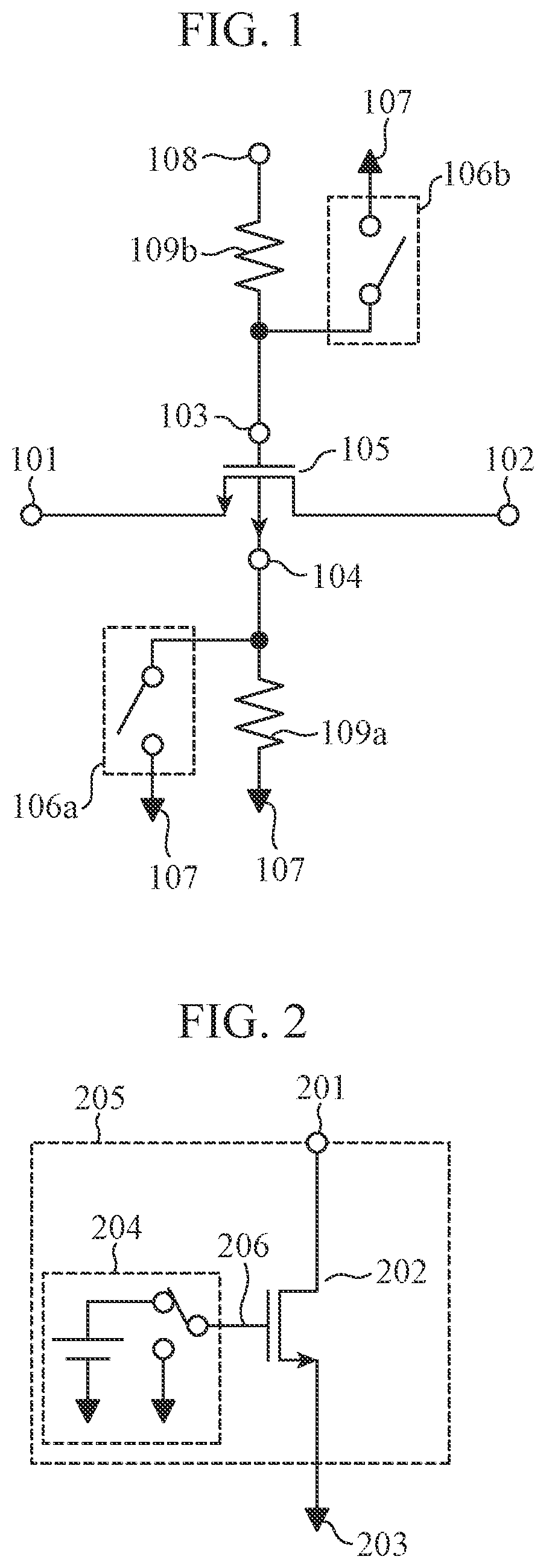
[0015]FIG. 1 is a configuration diagram of a high-frequency switch of the present embodiment.

[0016]The high-frequency switch of the present embodiment includes an NMOS transistor 105 having a source 101, a drain 102, a gate 103, and a back gate 104; resistive elements 109b and 109a for biasing the gate 103 and the back gate 104; and a first switching circuit 106a and a second switching circuit 106b. The gate 103 is connected to a gate control terminal 108 through the resistive element 109b, and the back gate 104 is connected to a high-frequency ground 107 through the resistive element 109a. The first switching circuit 106a is connected in parallel with the resistive element 109a between the back gate 104 and the high-frequency ground 107. The second switching circuit 106b is connected in parallel with the resistive element 109b between the gate 103 and the high-frequency ground 107.

[0017]The NMOS transistor 105 which is most widely used as a high-frequency switch performs electrical...

second embodiment

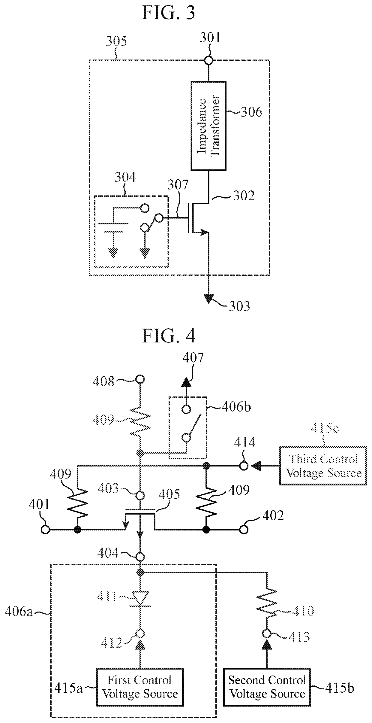
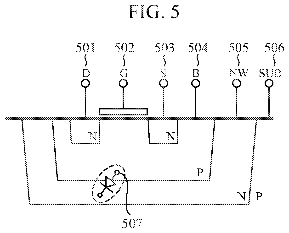
[0027]FIG. 4 is a configuration diagram of a high-frequency switch according to a second embodiment. FIG. 5 is a cross-sectional view of a transistor of the high-frequency switch of the second embodiment.

[0028]The high-frequency switch of the second embodiment includes an NMOS transistor 405 having a source 401, a drain 402, a gate 403, and a back gate 404; a resistive element 409 for biasing the gate 403; and a first switching circuit 406a and a second switching circuit 406b. Here, the NMOS transistor 405 having the source 401, the drain 402, the gate 403, and the back gate 404 is the same as the NMOS transistor 105 having the source 101, the drain 102, the gate 103, and the back gate 104 of the first embodiment. In addition, the resistive element 409 and a gate control terminal 408 which are connected to the gate 403 are the same as the resistive element 109b and the gate control terminal 108 of the first embodiment.

[0029]In addition, the first switching circuit 406a of the second...


PUM


Abstract

An NMOS transistor performs electrical conduction or cut-off between a drain and a source by controlling a potential at a gate. A resistive element is connected between a back gate of the NMOS transistor and a high-frequency ground. A first switching circuit is disposed in parallel with the resistive element between the back gate and the high-frequency ground and causes a short circuit between the back gate and the high-frequency ground upon cut-off.

Description

TECHNICAL FIELD[0001]The present invention relates to a high-frequency switch using a semiconductor switch.BACKGROUND ART[0002]For a high-frequency switch used in a radio communication device, there is known a high-frequency switch using a field effect transistor (FET) which is manufactured by a triple-well process. The basic operation of the high-frequency is such that a signal between a source and a drain is used to switch between conduction and cut-off states by applying a control voltage to a gate.[0003]When a high-frequency signal is applied to the high-frequency switch, a voltage at the source or drain changes over time on the basis of the amplitude of the input signal. At this time, when the gate or a back gate is biased at a fixed potential, Vgs (source-gate voltage) or Vgb (back gate-gate voltage) of the FET changes over time due to a change in voltage at the source or drain, which is a cause of signal distortion. Hence, conventionally, there is a configuration in which a r...

Claims


Application Information

Patent Timeline
Patent Type & Authority Applications(United States)
IPC IPC(8): H03K17/16
CPCH03K17/161H03K17/687H03K2017/066H03K17/063H03K2217/0018H03K2217/0054
Inventor FUJIWARA, TAKANOBUSHIMOZAWA, MITSUHIRO
Owner MITSUBISHI ELECTRIC CORP
Why Eureka
Try Eureka