Dielectric material, device comprising dielectric material, and method of preparing dielectric material
Pending Publication Date: 2021-07-01
SAMSUNG ELECTRONICS CO LTD
View PDF0 Cites 0 Cited by
- Summary
- Abstract
- Description
- Claims
- Application Information
AI Technical Summary
Benefits of technology
[0005]However, in the manufacture of a multi-layered ceramic capacitor (MLCC), which is a kind of miniaturized and thinned capacitor with large capacity, reduc
Problems solved by technology
In such a reductive sintering process, structural defects of the dielectric material may
Method used
View moreImage
Smart ImageViewing Examples

Examples
 PUM
| Property | Measurement | Unit |
|---|---|---|
| Temperature | aaaaa | aaaaa |
| Temperature | aaaaa | aaaaa |
| Temperature | aaaaa | aaaaa |
Abstract
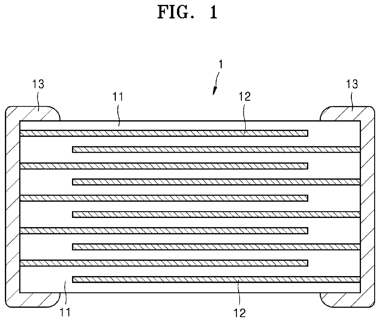
Provided are a dielectric material, a device including the dielectric material, and a method of preparing the dielectric material, in which the dielectric material may include: a layered perovskite compound, wherein the layered perovskite compound may include at least one selected from a Dion-Jacobson phase, an Aurivillius phase, and a Ruddlesden-Popper phase, a temperature coefficient of capacitance (TCC) of a capacitance at 200° C. with respect to a capacitance at 40° C. may be in a range of about −15 percent (%) to about 15%, and a permittivity of the dielectric material may be 200 or greater in a range of about 1 kilohertz (kHz) to about 1 megahertz (MHz).
Description
CROSS-REFERENCE TO RELATED APPLICATION[0001]This application claims the benefit of Korean Patent Application No. 10-2019-0178510, filed on Dec. 30, 2019, in the Korean Intellectual Property Office, the disclosure of which is incorporated herein in its entirety by reference.BACKGROUND1. Field[0002]The present disclosure relates to a dielectric material, a device including the dielectric material, and a method of preparing the dielectric material.2. Description of Related Art[0003]With the demands for continuous miniaturization, thinning, and large capacity of electronic devices, capacitors that may be further miniaturized and thinned, and have large capacity, as compared with existing capacitors, are required.[0004]In order to realize miniaturization, thinning, and large capacity of capacitors, a dielectric material that provides improved dielectric properties is required.SUMMARY[0005]However, in the manufacture of a multi-layered ceramic capacitor (MLCC), which is a kind of miniatur...
Claims
Login to View More Application Information
Patent Timeline
 IPC IPC(8): C30B1/02C03C17/23C03C17/00
CPCC30B1/023C03C17/23C04B2235/3258C04B2235/768C03C17/001C04B35/495C04B2235/3201C04B2235/3208C04B2235/3251C04B2235/442C04B2235/81C04B2235/652C04B2235/6581C04B2235/663C04B2235/6584C04B35/62675C01G33/006C01P2002/34C01P2002/72C01P2002/82H01B3/10H01G4/1209H01G4/30
Inventor KIM, HYUNGJUNKWAK, CHANSASAKI, TAKAYOSHIEBINA, YASUOLEE, CHANGSOOJUNG, DOHWONJO, GIYOUNGTANIGUCHI, TAKAAKI
Owner SAMSUNG ELECTRONICS CO LTD