Edge ring, substrate processing apparatus having the same and method of manufacturing semiconductor device using the apparatus

a substrate processing and edge ring technology, applied in the direction of chemical vapor deposition coating, coating, electric discharge tube, etc., can solve the problems of relatively poor deposition distribution/uniformity in the edge region, and the deposition at the bevel site may not be suppressed sufficiently, so as to improve the deposition characteristics

Pending Publication Date: 2021-07-01
SAMSUNG ELECTRONICS CO LTD
View PDF5 Cites 0 Cited by
  • Summary
  • Abstract
  • Description
  • Claims
  • Application Information

AI Technical Summary

Benefits of technology

[0010]Thus, the concentration distribution of the first portion and the second portion of the backside gas may be adjusted to provide improved deposition characteristics at a bevel site and an edge region of the wafer.

Problems solved by technology

However, in conventional edge rings, when the deposition suppression at the bevel site is relatively good, the deposition distribution / uniformity in the edge region may be deteriorated relatively or, conversely, when the deposition distribution / uniformity in the edge region is relatively good, the deposition at the bevel site may not be suppressed sufficiently.

Method used


Image

  • Edge ring, substrate processing apparatus having the same and method of manufacturing semiconductor device using the apparatus
  • Edge ring, substrate processing apparatus having the same and method of manufacturing semiconductor device using the apparatus
  • Edge ring, substrate processing apparatus having the same and method of manufacturing semiconductor device using the apparatus

Examples


Embodiment Construction

[0024]Hereinafter, example embodiments will be explained in detail with reference to the accompanying drawings.

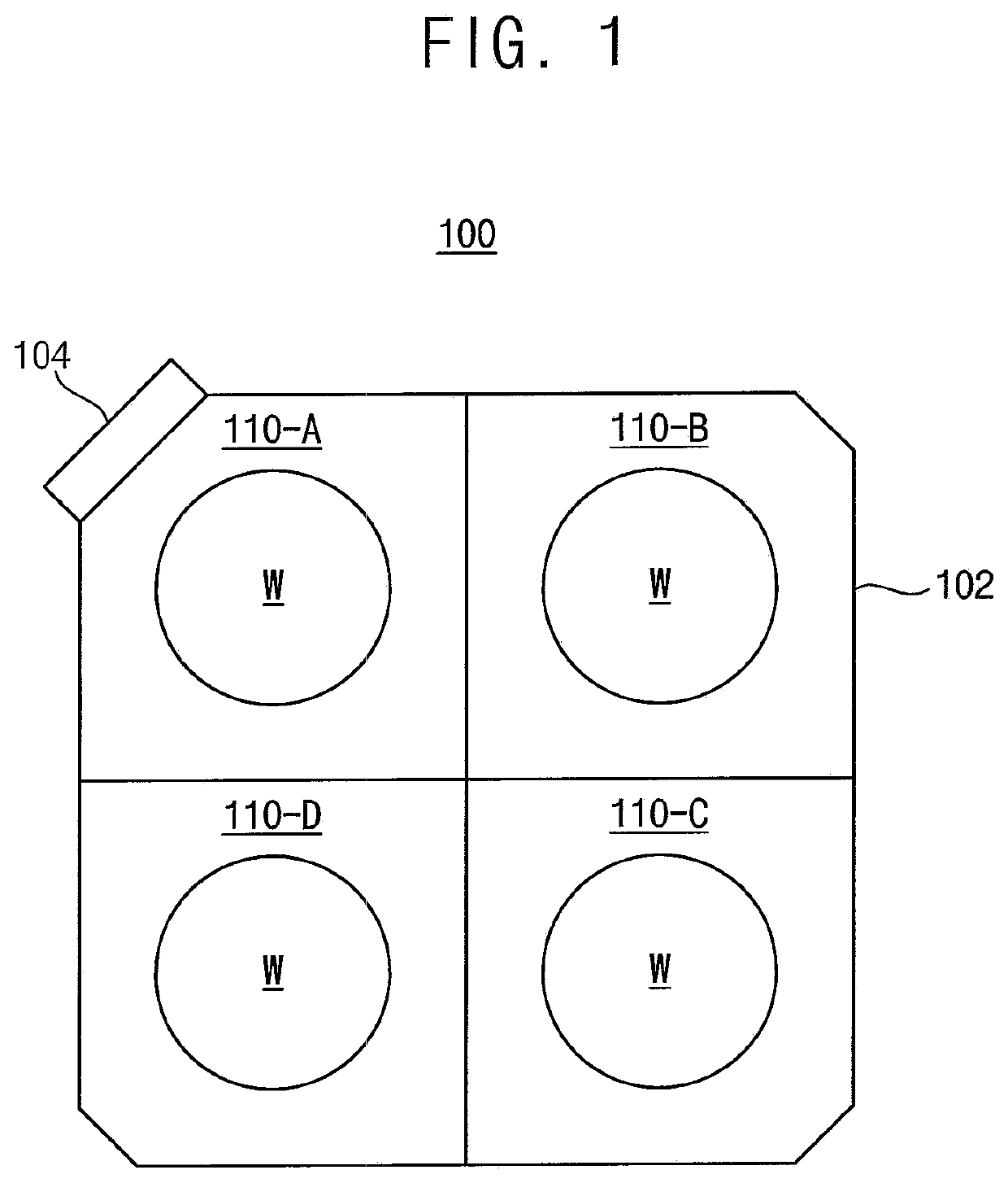
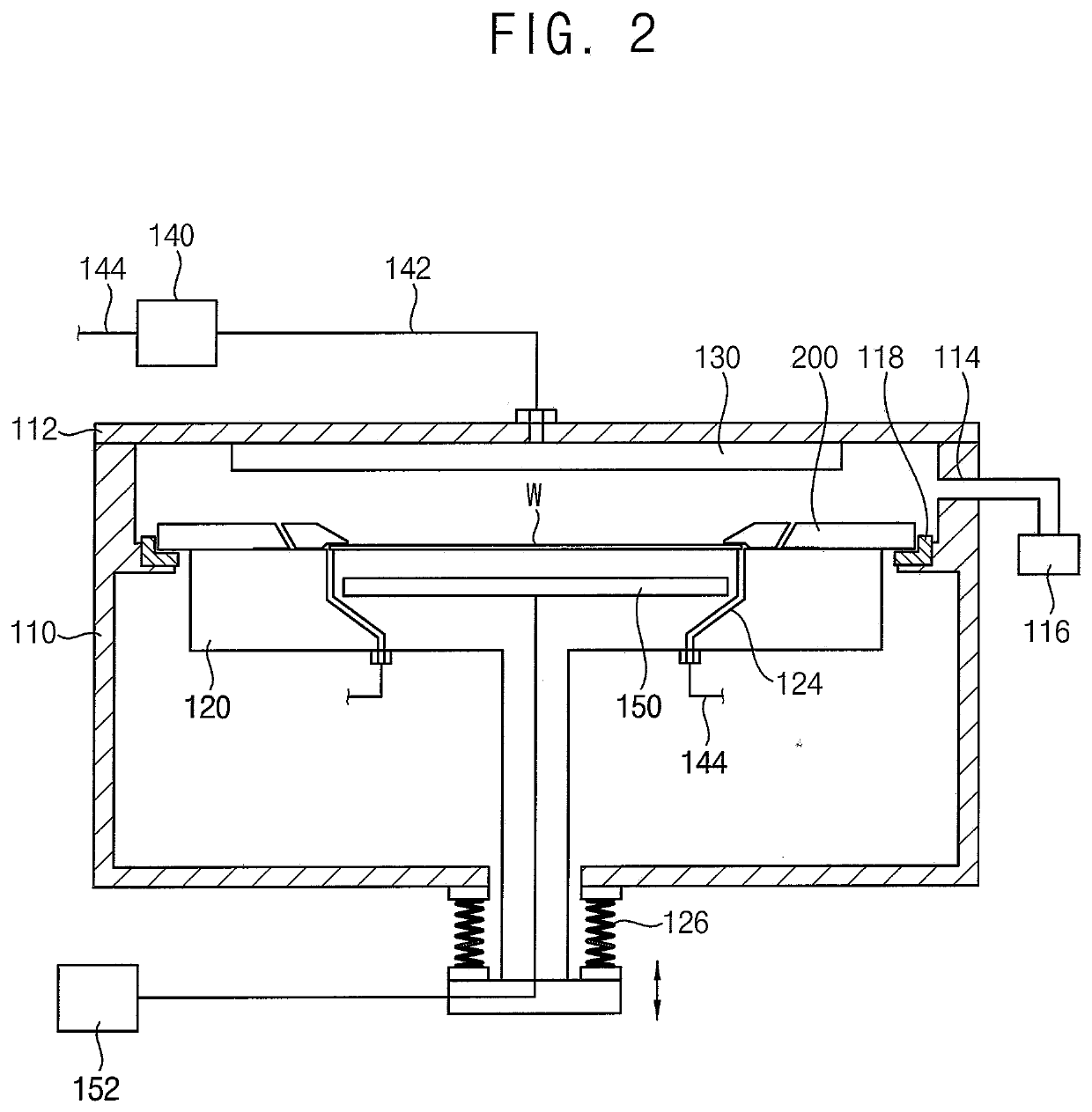
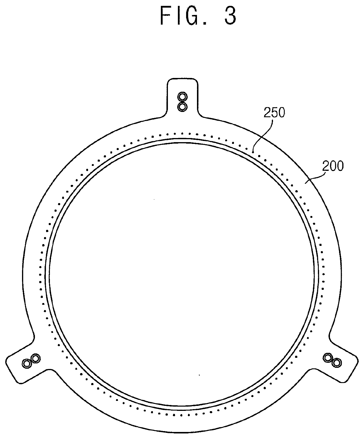
[0025]FIG. 1 is a plan view illustrating a substrate processing apparatus in accordance with example embodiments. FIG. 2 is a cross-sectional view illustrating a chamber of the substrate processing apparatus in FIG. 1. FIG. 3 is a plan view illustrating an edge ring mounted on a substrate stage of the substrate processing apparatus in FIG. 2.

[0026]Referring to FIGS. 1 to 3, a substrate processing apparatus 100 may include a plurality of chambers 110-A, 110-B, 110-C and 110-D which sequentially perform different processes. The substrate processing apparatus 100 may include sidewall partitions to divide a processing space into the chambers. At least one of the chambers may perform a selective layer deposition process on a wafer W using vapor deposition.

[0027]For example, processing in the chambers may be repeated one or more times, and each iteration may correspond to one ALD...


PUM

PropertyMeasurementUnit
angleaaaaaaaaaa
angleaaaaaaaaaa
angleaaaaaaaaaa

Abstract

An edge ring includes an annular body portion having a bottom surface and a top surface, a first step portion extending along an inner periphery of the body portion and having an annular first bottom surface positioned higher than the bottom surface of the body portion by a first height, an inclined portion extending along an inner periphery of the first step portion and having an inclined bottom surface extending at a first angle with respect to a first plane in which the first bottom surface is placed, a second step portion extending along an inner periphery of the inclined portion and having a second bottom surface positioned higher than the bottom surface of the body portion by a second height greater than the first height, and a plurality of passages extending outwardly from the first bottom surface of the first step portion at a second angle with respect to the first bottom surface.

Description

PRIORITY STATEMENT[0001]This application claims priority under 35 U.S.C. § 119 to Korean Patent Application No. 10-2019-0178956, filed on Dec. 31, 2019 in the Korean Intellectual Property Office (KIPO), the contents of which are herein incorporated by reference in their entirety.BACKGROUND1. Field[0002]Example embodiments relate to an edge ring and a substrate processing apparatus having the same. More particularly, example embodiments relate to an edge ring used for deposition distribution in an edge region of a wafer and a substrate processing apparatus having the same. The present disclosure also relates to a method of manufacturing semiconductor devices using the apparatus.2. Description of the Related Art[0003]An edge ring may be mounted on a substrate stage of a substrate processing apparatus for depositing a metal film, such as tungsten, on a wafer. The edge ring may be helpful in improving deposition distribution of the metal film in an edge region of the wafer. In an embodi...

Claims


Application Information

Patent Timeline
Patent Type & Authority Applications(United States)
IPC IPC(8): H01J37/32C23C16/458
CPCH01J37/32642C23C16/4585C23C16/4412C23C16/45597H01J37/32715H01L21/68735
Inventor LIM, HONGTAEKKIM, JUNGHYEONSHIN, SANGGONFEYGENSON, OLEGLEE, KYUHOHAN, DONGHOONHONG, KWANGPYO
Owner SAMSUNG ELECTRONICS CO LTD
Why Eureka
Try Eureka