
Photonic chip with buried laser source

a laser source and photonic chip technology, applied in the direction of lasers, semiconductor lasers, basic electric elements, etc., can solve the problem of difficulty in fabricating vias with an aspect ratio higher than 10/1, and achieve the effect of improving the dissipation of heat, and dissipating hea

Pending Publication Date: 2021-07-29
COMMISSARIAT A LENERGIE ATOMIQUE ET AUX ENERGIES ALTERNATIVES
View PDF4 Cites 1 Cited by
  • Summary
  • Abstract
  • Description
  • Claims
  • Application Information

AI Technical Summary

Benefits of technology

[0011]This chip has the advantage of being particularly simple to fabricate. However, it would be desirable, while retaining this advantage, to improve it even further by improving the thermal dissipation of the heat generated by the laser source while it is operating. To this end, the invention relates to such a photonic chip in which the photonic chip comprises an interconnect metal network forming a via that extends, in the optical layer, from the bonding interface to the first embedded electrical contact of the waveguide, this interconnect metal network comprising metal vias that electrically connect together metal lines that extend mainly parallel to the plane of the chip, these metal lines being arranged one above the other within the optical layer.

Problems solved by technology

Specifically, it is difficult to fabricate vias having an aspect ratio higher than 10 / 1.

Method used


Image

  • Photonic chip with buried laser source
  • Photonic chip with buried laser source
  • Photonic chip with buried laser source

Examples


first embodiment

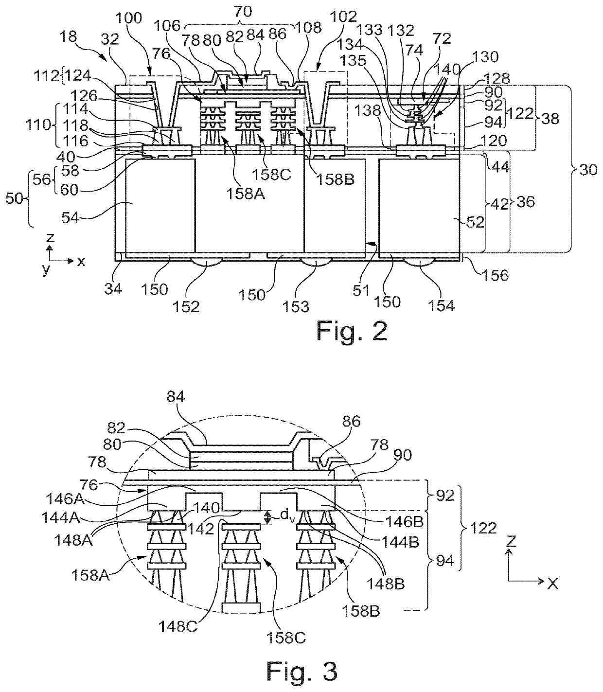
[0173]As a variant, the lower end of one or more of the vias 158A, 158B, 158C and 266 is electrically and mechanically connected to at least one primary via in order to improve the thermal dissipation of the heat produced by the laser source. Thus, in a first embodiment, the lower end of at least one of the vias 158A, 158B and 266 is electrically and mechanically connected to a primary via used to electrically connect one of the components of the chip 18 to the carrier 14. For example:[0174]the lower ends of the vias 158A and 158B are electrically and mechanically connected to the primary vias 50 and 51, respectively, or[0175]the lower ends of vias 158A and 158B are both electrically and mechanically connected to the primary via 50 or 51 or 52, or[0176]the lower end of via 266 is electrically and mechanically connected to the primary via 50 or 51 or 52.

second embodiment

In a second embodiment, the lower end of at least one of the vias 158A, 158B and 266 is electrically and mechanically connected to an additional primary via. This additional primary via is electrically isolated. It is therefore electrically isolated from the primary vias 50, 51 and 52. This additional primary via is therefore not used to make an electrical connection. For example, the lower end of via 158A or 158B is electrically and mechanically connected to such an additional primary via.

[0177]The diameter of one or more of the vias 158A, 158B, 158C and of the via 266 is not necessarily smaller than 3 μm or 1 μm. Its diameter may also be larger than these values.

[0178]The use of the vias 158A, 158B, 158C and 266 to improve the dissipation of the heat produced by a laser source applies similarly to the improvement of the dissipation of the heat produced by any type of optical or electronic component at least one portion of which is embedded in the sublayer 122. For example, a via s...


PUM

PropertyMeasurementUnit
thicknessaaaaaaaaaa
distanceaaaaaaaaaa
distanceaaaaaaaaaa

Abstract

A photonic chip includes an optical layer bonded, via a bonding interface, to a carrier, and a laser source having a waveguide encapsulated in an encapsulating sublayer of the optical layer, the waveguide having a first electrical contact embedded in the encapsulating sublayer. The photonic chip also includes an interconnect metal network forming a via that extends, in the optical layer, from the bonding interface to the first embedded electrical contact of the waveguide, the interconnect metal network having metal vias that electrically connect to one another metals lines that extend mainly parallel to the plane of the chip, the metal lines being arranged one above the other within the optical layer.

Description

[0001]The invention relates to a photonic chip comprising a buried laser source and to a process for fabricating such a photonic chip.[0002]The photonic chips essentially lie in a plane called the “plane of the chip” below.[0003]Known photonic chips comprise:[0004]a substrate having upper and lower faces parallel to the plane of the chip, this substrate comprising, between the upper and lower faces:[0005]a carrier of thickness larger than 50 μm, this carrier being devoid of optical component,[0006]an optical layer bonded, via a bonding interface, to the carrier, this optical layer comprising, in succession, from the upper face to the bonding interface:[0007]an oxide sublayer, and[0008]an encapsulating sublayer,[0009]a laser source buried in the optical layer, this laser source comprising a waveguide that is produced on the side of the oxide sublayer which faces the bonding interface and that is encapsulated in a dielectric material of the encapsulating layer, this waveguide comprisi...

Claims


Application Information

Patent Timeline
Patent Type & Authority Applications(United States)
IPC IPC(8): H01S5/026H01S5/12H01S5/022H01S5/11
CPCH01S5/026H01S5/11H01S5/022H01S5/12H01S5/02325H01S5/02345H01L23/49827H01L27/15H01L33/62H01L2224/16225H01L2924/15311H01L2924/15192H01S5/04257H01S5/02469H01S5/023
Inventor MENEZO, SYLVIECHERAMY, SÉVERINE
Owner COMMISSARIAT A LENERGIE ATOMIQUE ET AUX ENERGIES ALTERNATIVES
Learn More