Photonic Circuit With Integrated Light Coupler

a photonic circuit and light coupler technology, applied in the field of photonic integrated circuits, can solve the problems of large constraints on the choice of imagers, adversely affecting the signal to noise ratio, and each grating coupler may typically have a low out-coupling efficiency, so as to achieve good and efficient light coupling

Active Publication Date: 2021-09-23
INTERUNIVERSITAIR MICRO ELECTRONICS CENT (IMEC VZW) +1
View PDF0 Cites 0 Cited by
  • Summary
  • Abstract
  • Description
  • Claims
  • Application Information

AI Technical Summary

Benefits of technology

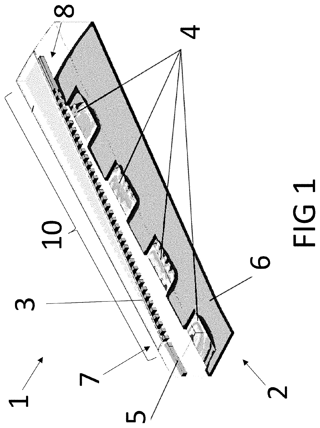
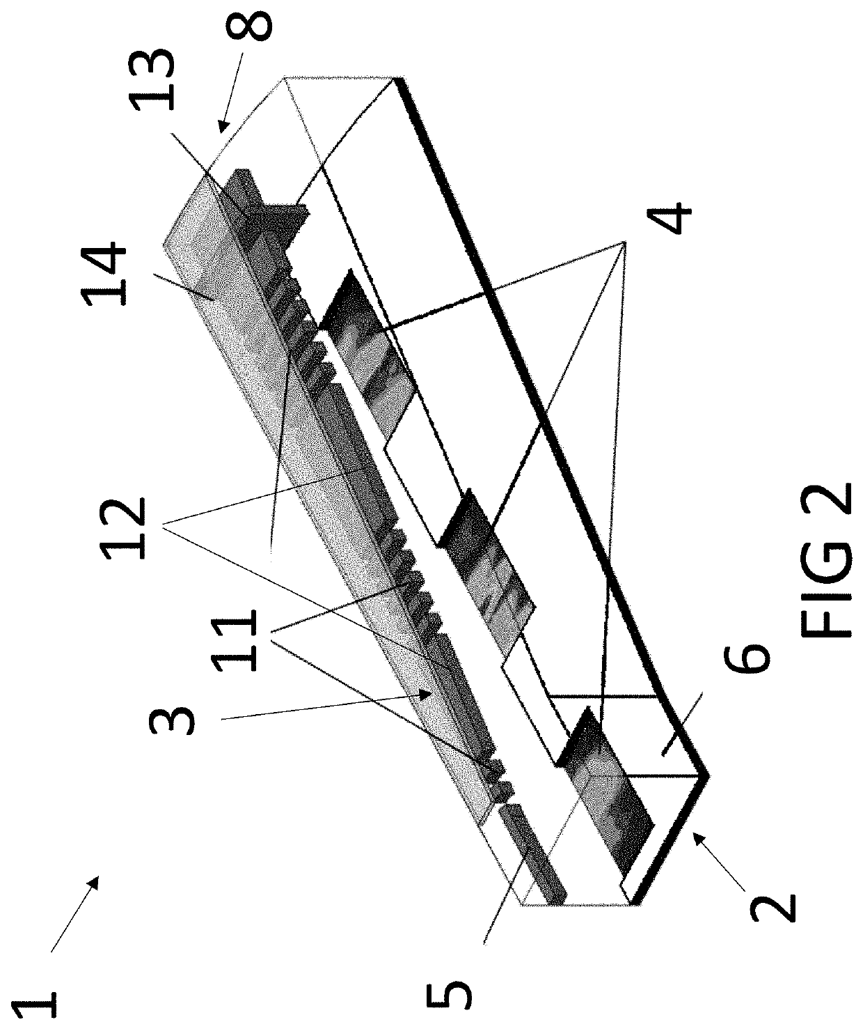
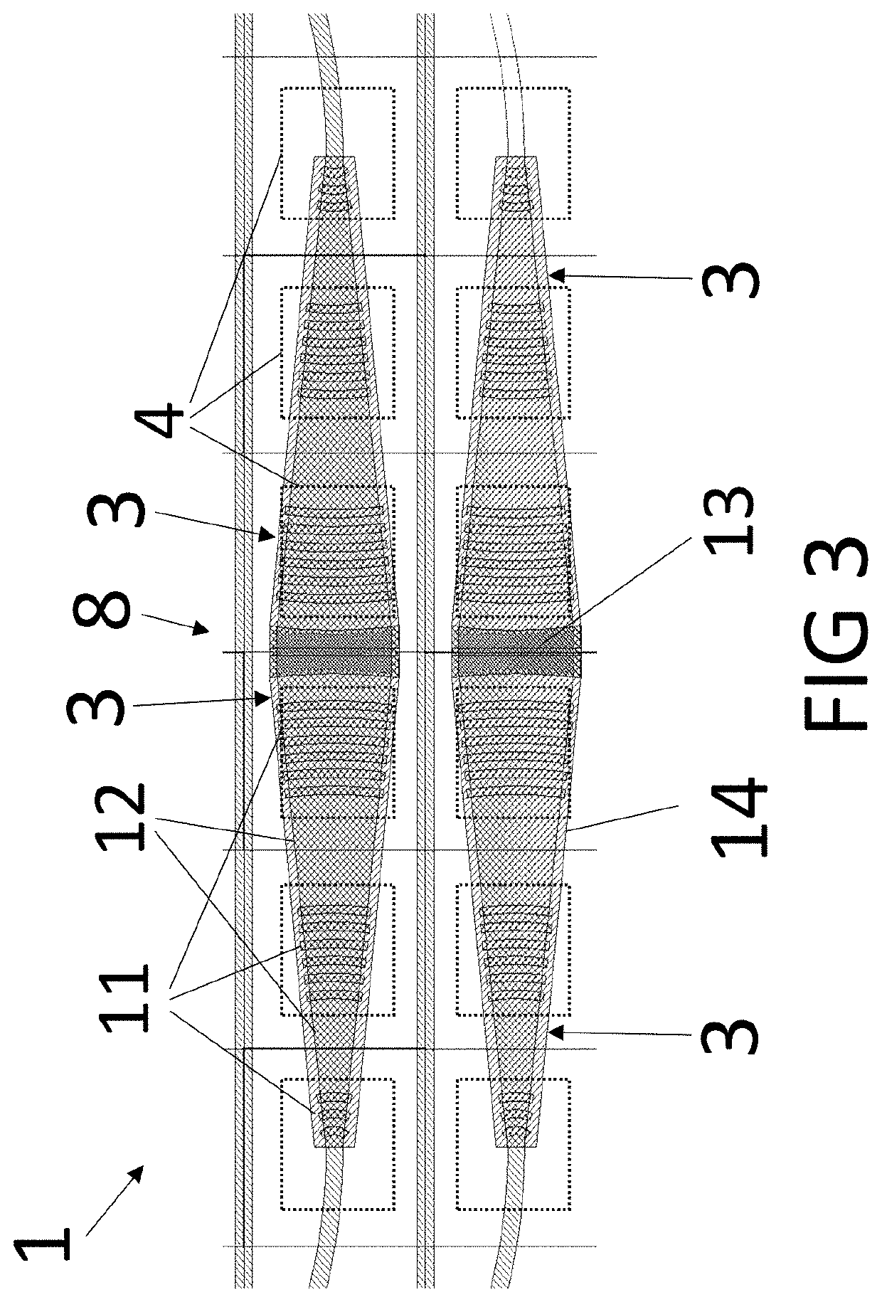
[0007]It is an object of embodiments of the present invention to provide good and efficient coupling of light from an integrated waveguide to an image detector.
[0009]It is an advantage of embodiments of the present invention that efficiency of light detection may be increased, e.g. relative to a prior art integrated photonic device for coupling light from a waveguide to an image detector.
[0010]It is an advantage of embodiments of the present invention that noise, such as dark current and read noise, generated in quantifying a light signal, e.g. in spectral analysis of the light signal, can be reduced.
[0014]In an integrated photonic device in accordance with embodiments of the present invention, each of the light guiding segments may be adapted for guiding the light signal between an adjacent pair of the diffraction gratings without thereby diffracting light out of the light guiding segment.

Problems solved by technology

However, it is a disadvantage of such prior-art systems that each grating coupler may typically have a low out-coupling efficiency.
Furthermore, this may adversely affect the signal to noise ratio for the signal detected by the individual pixels.
This may put large constraints on the choice of imager from commercially available imaging solutions, or might even require the development of expensive custom arrays.

Method used


Image

  • Photonic Circuit With Integrated Light Coupler
  • Photonic Circuit With Integrated Light Coupler
  • Photonic Circuit With Integrated Light Coupler

Examples


Embodiment Construction

[0039]The present invention will be described with respect to particular embodiments and with reference to certain drawings but the invention is not limited thereto but only by the claims. The drawings described are only schematic and are non-limiting. In the drawings, the size of some of the elements may be exaggerated and not drawn on scale for illustrative purposes. The dimensions and the relative dimensions do not correspond to actual reductions to practice of the invention.

[0040]Furthermore, the terms first, second and the like in the description and in the claims, are used for distinguishing between similar elements and not necessarily for describing a sequence, either temporally, spatially, in ranking or in any other manner. It is to be understood that the terms so used are interchangeable under appropriate circumstances and that the embodiments of the invention described herein are capable of operation in other sequences than described or illustrated herein.

[0041]Moreover, t...


PUM

PropertyMeasurementUnit
areaaaaaaaaaaa
lengthaaaaaaaaaa
distanceaaaaaaaaaa

Abstract

An integrated photonic device may include an image detector that comprises an array of pixels. The device may further include an integrated waveguide and a light coupler comprising a light receiving part optically coupled to the integrated waveguide for receiving a light signal. The light coupler may be adapted for coupling a same predetermined spectral band of the light signal to each of a plurality of pixels of the image detector. The light coupler may include a tapered portion, in which the light coupler tapers outward in a direction of propagation, and an end part comprising an elliptically shaped back reflector for reflecting light propagating along the direction of propagation back through the light coupler toward the integrated waveguide.

Description

FIELD OF THE INVENTION[0001]The invention relates to the field of photonic integrated circuits. More specifically it relates to an integrated photonic device, and related method, by which a light signal can be coupled from an integrated waveguide to an image detector.BACKGROUND OF THE INVENTION[0002]In integrated photonic devices known in the art, such as integrated spectrometers, a photonic circuit may be provided on an image detector. For example, a plurality of grating couplers may couple light from a waveguide towards an image detector for detection.[0003]For example, U.S. Pat. No. 6,226,083 discloses an integrated-optic spectrometer for analysing the composition of light reflected off a sample under analysis. The integrated-optic spectrometer comprises a waveguide, fabricated onto an oxidized substrate, and an array of diffraction gratings and a detector array. The detector array is mounted on the waveguide so as to receive the light of different wavelengths diffracted by the g...

Claims


Application Information

Patent Timeline
Patent Type & Authority Applications(United States)
IPC IPC(8): G02B6/122G01J3/02G01J3/18
CPCG02B6/1228G01J3/0259G01J3/1895G01J3/021G02B6/0035G02B6/0083G02B6/122
Inventor CLAES, TOM
Owner INTERUNIVERSITAIR MICRO ELECTRONICS CENT (IMEC VZW)
Why Eureka
Try Eureka