Method for forming amorphous silicon thin film, method for manufacturing semiconductor device including same, and semiconductor manufactured thereby

a technology of amorphous silicon and amorphous silicon, which is applied in the direction of coating, chemical vapor deposition coating, metallic material coating process, etc., can solve the problems of product productivity decline, poor layer, and formation of adhesion state of a-si layer, so as to reduce the total number of processes, reduce the occurrence of etching, and improve the etching profile

Active Publication Date: 2021-12-23
WONIK IPS CO LTD
View PDF3 Cites 0 Cited by
  • Summary
  • Abstract
  • Description
  • Claims
  • Application Information

AI Technical Summary

Benefits of technology

[0021]A method for depositing a thin film according to the present invention and a thin film using the same have advantages in that in depositing an a-Si thin film on a SiN thin film, a first step of forming a first amorphous silicon layer is performed using a first gas containing silicon such as SiH4 and a second gas containing nitrogen such as NH3, and then a second step of forming a second amorphous silicon layer made of such as a-Si is performed using only a gas containing silicon such as SiH4, so that an a-Si layer may be formed with reduced occurrence of a tail phenomenon on the SiN thin film without additionally performing a plasma treatment process.
[0022]In addition, the method for depositing a thin film according to the present invention and the thin film using the same have advantages in that in depositing an a-Si thin film on a SiN thin film, the ratio of the supply flow rate of the first gas and the ratio of the supply flow rate of the second gas in the above-described first step may be adjusted, so that the density of a thin film formed on a substrate may be controlled. As a result, an etch rate in a lower region of the thin film is increased, thereby improving etch profile.
[0023]In addition, the method for depositing a thin film according to the present invention and the thin film using the same have advantages in that in depositing an a-Si thin film on a SiN thin film, a plasma treatment process using NH3 is omitted, so that a total number of processes is reduced, thereby improving productivity.

Problems solved by technology

However, due to the difference in film quality and roughness of the SiN base layer, the adhesion state of the a-Si layer formed on the SiN base layer may be poor, and when an etching process for the a-Si layer is performed, there is a problem in that a tail phenomenon occurs in which the etching of a lower region (210a in FIG. 3) of the a-Si layer is relatively insufficient.
However, there is a problem with the prior art in that due to the increase in the number of process steps caused by the performance of the NH3 plasma treatment process before depositing a-Si, product productivity decreases, and due to frequent power on / off, the possibility of particle generation on an a-Si thin film increases.

Method used


Image

  • Method for forming amorphous silicon thin film, method for manufacturing semiconductor device including same, and semiconductor manufactured thereby
  • Method for forming amorphous silicon thin film, method for manufacturing semiconductor device including same, and semiconductor manufactured thereby
  • Method for forming amorphous silicon thin film, method for manufacturing semiconductor device including same, and semiconductor manufactured thereby

Examples


Embodiment Construction

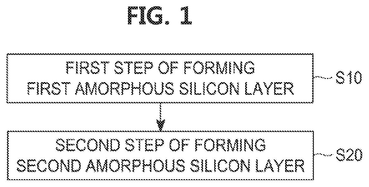
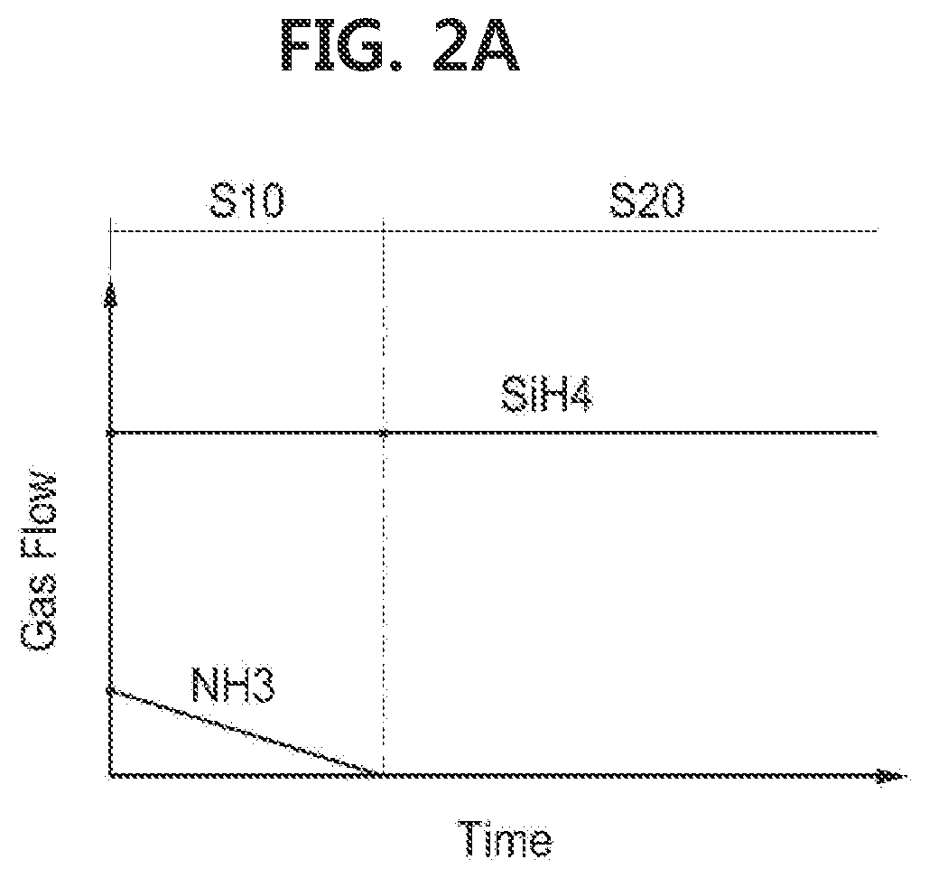
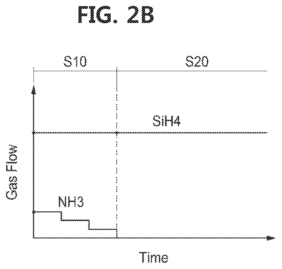
[0035]Hereinafter, a method for forming an amorphous silicon thin film, a method for manufacturing a semiconductor device including the same, and a semiconductor device manufactured thereby, all according to the present invention, will be described with reference to the accompanying drawings.

[0036]The method for forming an amorphous silicon thin film according to the present invention includes First step S10 of providing a first gas containing silicon and a second gas containing nitrogen on a substrate 100 to form a first amorphous silicon layer 310b, and Second step S20 of providing a first gas containing silicon on the substrate 100 having the first amorphous silicon layer 310b formed thereon to form a second amorphous silicon layer 300a.

[0037]Here, the substrate 100 is a substrate constituting a device such as an LCD substrate, an OLED substrate, and the like manufactured through a semiconductor process, and any substrate may be used as long as it is a substrate having a SiN lay...


PUM

PropertyMeasurementUnit
supply flow rateaaaaaaaaaa
flow rateaaaaaaaaaa
roughnessaaaaaaaaaa

Abstract

The present invention relates to a method for forming an amorphous silicon thin film, a method for manufacturing a semiconductor device including the same, and a semiconductor device manufactured thereby. The present invention discloses a method for forming an amorphous silicon thin film, wherein the method includes a first step (S10) of providing a first gas containing silicon and a second gas containing nitrogen on a substrate (100) to form a first amorphous silicon layer (310b), and a second step (S20) of providing a first gas containing silicon on the substrate (100) having the first amorphous silicon layer (310b) formed thereon to form a second amorphous silicon layer (300a).

Description

CROSS-REFERENCE TO RELATED APPLICATIONS[0001]This U.S. non-provisional patent application claims priority under 35 U.S.C. § 119 of Korean Patent Application No. 10-2020-0075232, filed on Jun. 19, 2020, the entire contents of which are hereby incorporated by reference.FIELD OF THE INVENTION[0002]The present invention disclosed herein relates to a method for forming an amorphous silicon thin film, a method for manufacturing a semiconductor device including the same, and a semiconductor device manufactured thereby.BACKGROUND ART[0003]Devices such as semiconductors, LCD substrates, MED substrates, and the like are manufactured by a semiconductor process including one or more deposition processes and etching processes.[0004]For example, a substrate constituting a device may have a second amorphous silicon layer 300a, that is, an a-Si layer. Also, in order to facilitate the deposition of the a-Si layer on a substrate 100, it is preferable that a base layer of such as SiO2 or SiN is first ...

Claims


Application Information

Patent Timeline
Patent Type & Authority Applications(United States)
IPC IPC(8): H01L21/02
CPCH01L21/0262H01L21/02532H01L21/0245H01L21/02592H01L21/0257H01L21/02488H01L21/02502H01L21/0251H01L21/02513C23C16/24C23C16/0272
Inventor MOON, JAE JUNGCHOI, YOUNG CHULKIM, DONG HAK
Owner WONIK IPS CO LTD
Why Eureka
Try Eureka