Optical element and wafer level optical module

a technology of optical elements and wafers, applied in the field of optical elements and can solve the problems of difficult miniaturization of wlo modules, and achieve the effect of improving the integration degree of wafer level optical modules and more optical functionality

Active Publication Date: 2022-02-17
HIMAX TECH LTD
View PDF8 Cites 0 Cited by
  • Summary
  • Abstract
  • Description
  • Claims
  • Application Information

AI Technical Summary

Benefits of technology

[0005]The disclosure provides a wafer level optical module with high integration and better functionality.
[0026]Based on the above, in the optical element and the wafer level optical module according to an embodiment of the disclosure, two optical films are disposed between two substrates. A gap is included between the two substrates through the arrangement of the spacer. Each of the optical films has a plurality of optical microstructures which are disposed in the gap. The plurality of optical microstructures of one of the two optical films does not overlap the plurality of optical microstructures of the other of the two optical films so that the optical element can be provided with more optical functionality. Accordingly, the integration degree of the wafer level optical module can also be improved.

Problems solved by technology

However, along with increasing demand on optical functionality of the electronic product, the number of optical components (for example, dot projector, flood illuminator and proximity sensor) adopted in the WLO module inevitably increases, so that the miniaturization of the WLO module becomes more difficult due to the increasing structural complexity.

Method used


Image

  • Optical element and wafer level optical module
  • Optical element and wafer level optical module
  • Optical element and wafer level optical module

Examples


first embodiment

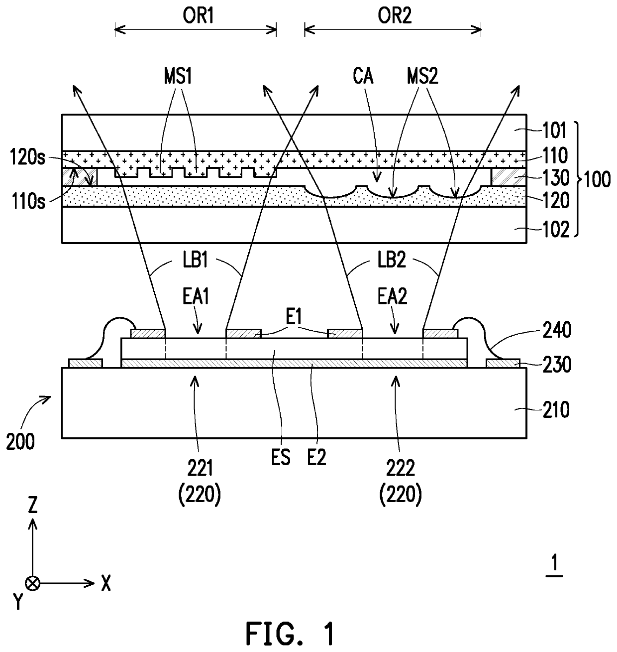
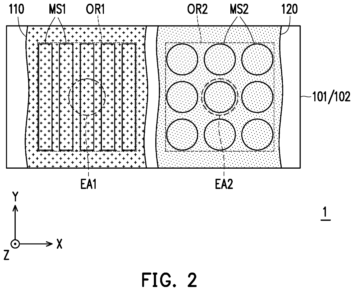
[0039]FIG. 1 is a schematic cross-sectional view of a wafer level optical module according to the invention. FIG. 2 is a schematic top view of the wafer level optical module in FIG. 1. In particular, for clear presentation and explanation, FIG. 2 omits the illustration of spacer 130, first electrode E1, second electrode E2, epitaxial structure ES, circuit substrate 210, pad 230 and bonding wire 240 of FIG. 1.

[0040]Referring to FIG. 1 and FIG. 2, a wafer level optical module includes an optical element 100 and a light emitter 200. The optical element 100 is arranged on the optical path of the light emitter 200. Specifically, the light emitter 200 has a plurality of light exiting apertures, for example, a light exiting aperture EA1 and a light exiting aperture EA2. The optical element 100 is overlapped with these light exiting apertures. For example, in the present embodiment, the optical element 100 has a first optical region OR1 and a second optical region OR2. It should be noted th...

second embodiment

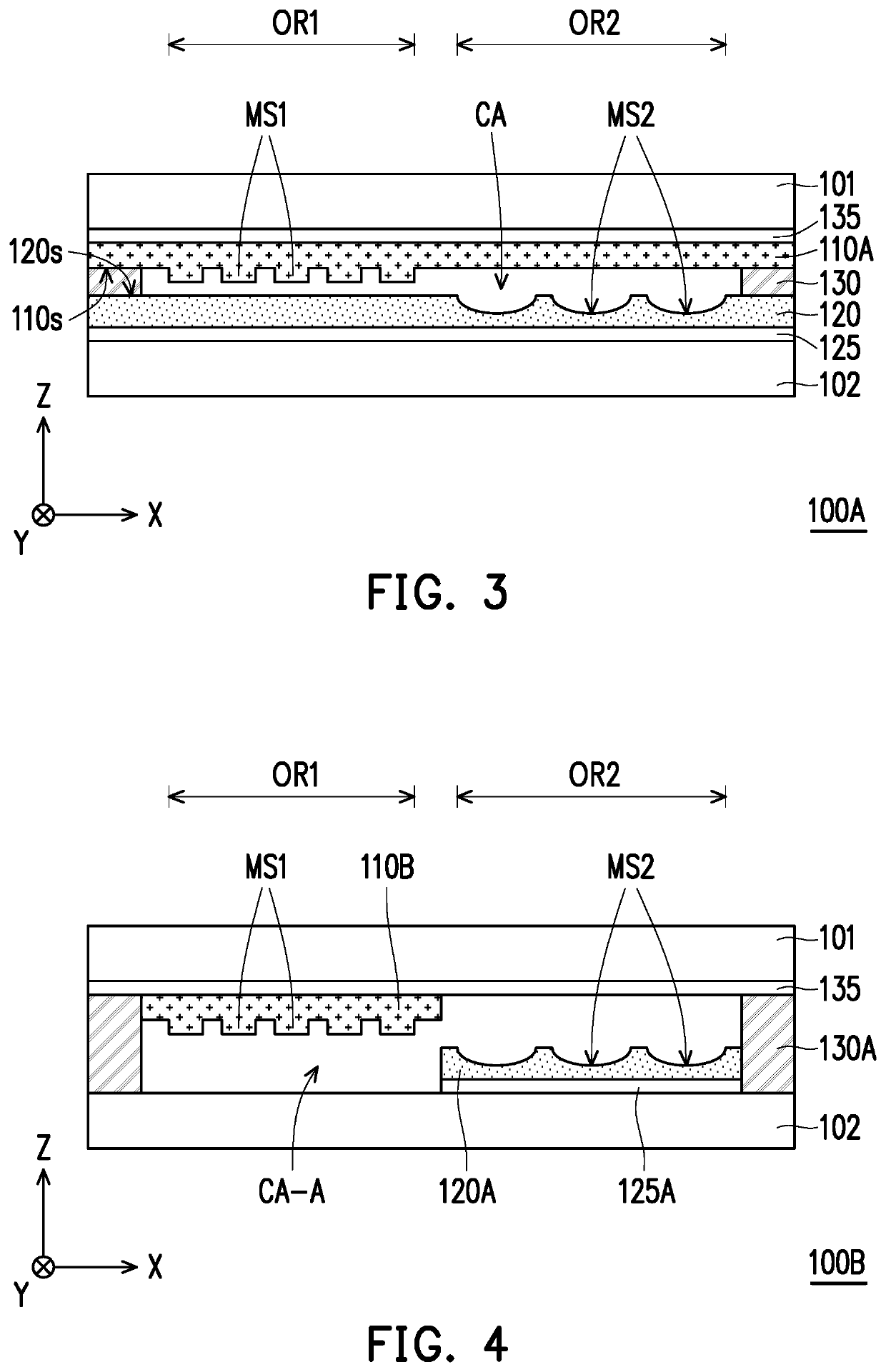
[0054]FIG. 3 is a schematic cross-sectional view of an optical element according to the invention.

[0055]Referring to FIG. 3, the difference between the optical element 100A of the present embodiment and the optical element 100 of FIG. 1 lies in the composition of the optical element. In the present embodiment, the optical element 100A further includes an index matching layer 135 and a buffer layer 125. The index matching layer 135 is disposed between the first substrate 101 and the first optical film 110A. The buffer layer 125 is disposed between the second substrate 102 and the second optical film 120. Due to the refractive index of the first optical film 110A is high (for example, the refractive index is greater than 1.7), the reflection of the light beam at the interface between the first substrate 101 and the first optical film 110A can be inhibited by configuring the index matching layer 135. In the present embodiment, the width of the first optical microstructure MS1 or the pi...

third embodiment

[0057]FIG. 4 is a schematic cross-sectional view of an optical element according to the invention.

[0058]Referring to FIG. 4, the difference between the optical element 100B of the present embodiment and the optical element 100A of FIG. 3 lies in the configuration of the optical element. In the present embodiment, the spacer 130A is connected between the index matching layer 135 and the second substrate 102. The index matching layer 135, the second substrate 102 and the spacer 130A define a cavity CA-A of the optical element 100B. The first optical film 110B, the second optical film 120A and the buffer layer 125A are disposed in the cavity CA-A.

[0059]Particularly, the orthogonal projection of the first optical film 110B on the first substrate 101 does not overlap with the orthogonal projection of the second optical film 120A on the first substrate 101. For example, compared to the optical element 100A of FIG. 3, the manufacturing process of the optical element 100B may further includ...


PUM

PropertyMeasurementUnit
widthaaaaaaaaaa
widthaaaaaaaaaa
widthaaaaaaaaaa

Abstract

An optical element including a first substrate, a second substrate, a first optical film, a second optical film, and a spacer is provided. The first optical film is disposed on the first substrate and has a first surface and a plurality of first optical microstructures. The first optical microstructures are disposed on the first surface. The second optical film is disposed on the second substrate and has a second surface and a plurality of second optical microstructures. The second surface is opposite to the first surface. The second optical microstructures are disposed on the second surface. The orthogonal projection of the first optical microstructures on the first substrate does not overlap with the orthogonal projection of the second optical microstructures on the first substrate. The spacer is disposed between the first substrate and the second substrate. A wafer level optical module adopting the optical element is also provided.

Description

BACKGROUNDTechnical Field[0001]The invention relates to optical element and optical module, and in particular, to an optical element and a wafer level optical module.Description of Related Art[0002]In recent years, along with a trend of module miniaturization and low price of electronic products, a wafer level module (WLM) technique draws attention. The WLM technique is mainly to use a wafer level fabrication technique to miniaturize a volume of the electronic product and decrease the cost thereof. For example, when the aforementioned technique is applied to fabricate wafer level optical (WLO) lens modules, the WLO lens modules may have smaller volume compares with that of a conventional lens module, so that the WLO lens modules can be applied to camera modules of, for example, mobile phones.[0003]However, along with increasing demand on optical functionality of the electronic product, the number of optical components (for example, dot projector, flood illuminator and proximity sens...

Claims


Application Information

Patent Timeline
Patent Type & Authority Applications(United States)
IPC IPC(8): G02B5/20B29D11/00
CPCG02B5/20B29D11/00634H01S5/423H01S5/06H01S5/005B29D11/00307H01L33/58H01L27/153
Inventor CHANG, CHIH-SHENGTSAI, MENG-KOHUANG, TENG TE
Owner HIMAX TECH LTD
Why Eureka
Try Eureka