Transmission line and electronic device
a technology of electronic devices and transmission lines, applied in waveguide devices, non-metallic protective coating applications, waveguide types, etc., can solve the problems of affecting the operation of the device. , to achieve the effect of reducing or preventing unwanted coupling and increasing the size of the external connection portion
- Summary
- Abstract
- Description
- Claims
- Application Information
AI Technical Summary
Benefits of technology
Problems solved by technology
Method used
Image
Examples
first preferred embodiment
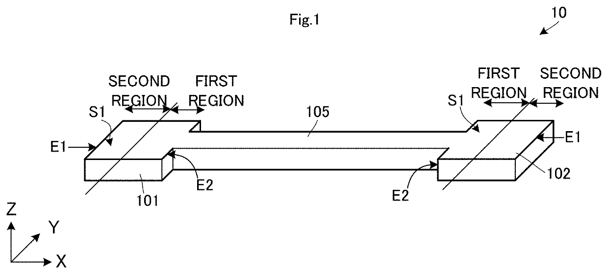
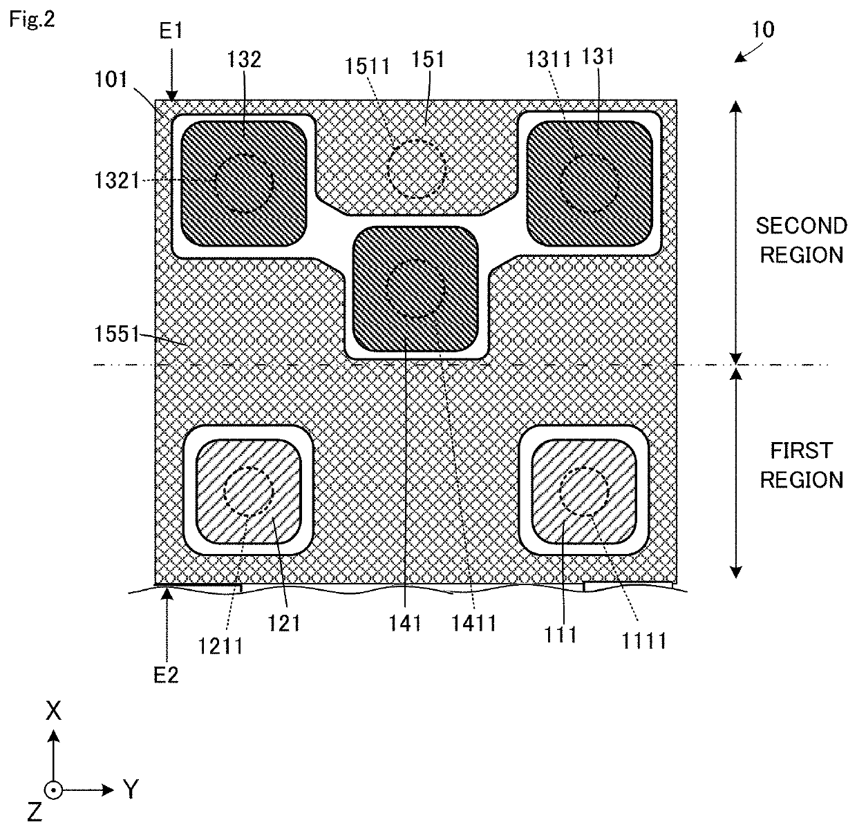
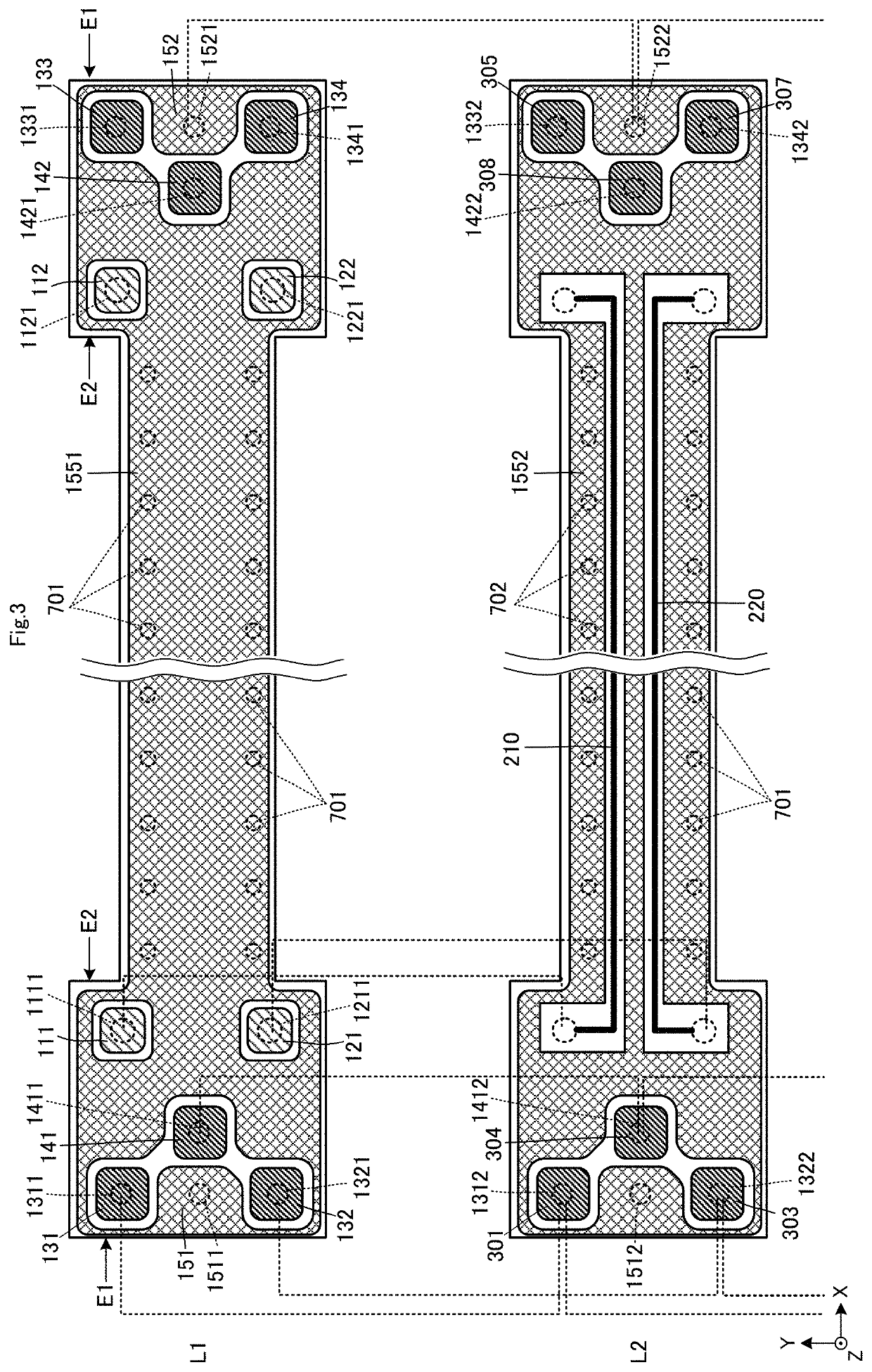
[0025]FIG. 1 is an external perspective view of a transmission line 10 according to a first preferred embodiment of the present invention. FIG. 2 is a plan view showing an external connection portion 101 of the transmission line 10 according to the first preferred embodiment. FIG. 3 is an exploded plan view of a first layer L1 and a second layer L2 in the transmission line 10 according to the first preferred embodiment. FIG. 4 is an exploded plan view of a third layer L3 and a fourth layer L4 in the transmission line 10 according to the first preferred embodiment. FIG. 5 is an exploded plan view of a fifth layer L5 in the transmission line 10 according to the first preferred embodiment. FIG. 6 is a cross-sectional view of the external connection portion 101 of the transmission line 10. FIG. 7 is a plan view showing an overview of a protective layer 600 provided on the external connection portion 101 according to the first preferred embodiment. FIG. 8 is an external view of an electr...
second preferred embodiment
[0107]A transmission line according to a second preferred embodiment of the present invention will be described with reference to the drawings. FIG. 9 is a plan view showing an external connection portion 101 of a transmission line 10A according to the second preferred embodiment of the present invention. FIG. 10 is an exploded plan view of a first layer L1 and a second layer L2 in the transmission line 10A according to the second preferred embodiment. FIG. 11 is an exploded plan view of a third layer L3 and a fourth layer L4 in the transmission line 10A according to the second preferred embodiment. It is to be noted that, in FIG. 10, in order to make the drawing easy to see, the interlayer connection conductor 704 in the fifth layer L5 and the fourth layer L4 is omitted.
[0108]The transmission line 10A according to the present preferred embodiment is different from the transmission line 10 according to the first preferred embodiment in that third electrode pads 135 and 136 are provi...
third preferred embodiment
[0172]A transmission line according to a third preferred embodiment of the present invention will be described with reference to the drawings. FIG. 12A is a plan view showing an external connection portion 101B of a transmission line 10B according to the third preferred embodiment, FIG. 12B is a cross-sectional view of a first electrode pad 111, and FIG. 12C is a cross-sectional view of a third electrode pad 131.
[0173]The transmission line 10B according to the present preferred embodiment is different from the transmission line 10 according to the first preferred embodiment in that a width of the first electrode pads 111 and 112 and a width of the second electrode pads 121 and 122 are different from a width of the third electrode pads 131, 132, 133, 134, 135, 136, 137, and 138 and a width of the fourth electrode pads 141, 142, 145, and 146. Other configurations of the transmission line 10B are the same or substantially the same as the configurations of the transmission line 10 accor...
PUM
 Abstract
Description
Claims
Application Information


