Ceramic heater

Pending Publication Date: 2022-04-14
NGK INSULATORS LTD
View PDF0 Cites 0 Cited by
  • Summary
  • Abstract
  • Description
  • Claims
  • Application Information

AI Technical Summary

Benefits of technology

[0013]The ceramic heater of the present invention may include a side shield portion disposed so as to extend toward the wafer placement surface from an outer edge of the planar shield portion. Thus, the side shield portion prevents coupling between plasma that has flowed around to the side surface side of the ceramic plate and the heater electrode. It is therefore possible to prevent the occurrence of an abnormal condition (such as abnormal heat generation or abnormal expansion of the heater electrode) caused by such coupling. In this case, the side shield portion may be made of Al or an Al alloy. In this case, furthermore, the planar shield portion and the side shield portion may be embedded in the ceramic plate, and the side shield portion may have a distal end positioned between the wafer placement surface and the heater electrode. Thus, coupling between the plasma that has flowed around to the side surface side of the ceramic plate and the heater electrode can be reliably prevented.
[0014]In the ceramic heater of the present invention, the planar shield portion may be embedded in the ceramic plate, and a distance from the back surface to the planar shield portion may be larger than a distance from the wafer placement surface to the plasma electrode. The distance from the back surface to the planar shield portion affects plasma density on the wafer placement surface. Accordingly, setting the distance from the back surface to the plasma electrode to a large value can reduce the influence of the planar shield portion on the plasma on the wafer placement surface side. In addition, it is possible to easily prevent coupling between the plasma that has flowed around to the back surface side and the heater elect

Problems solved by technology

In such a ceramic heater, if a leakage current produced by the high-frequency voltage applied to the plasma electrode i

Method used


Image

  • Ceramic heater
  • Ceramic heater
  • Ceramic heater

Examples


Example

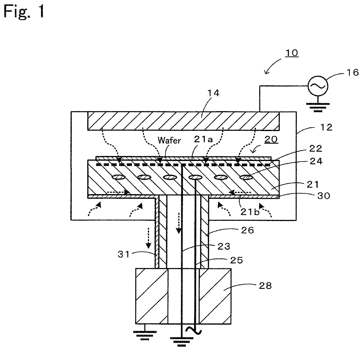
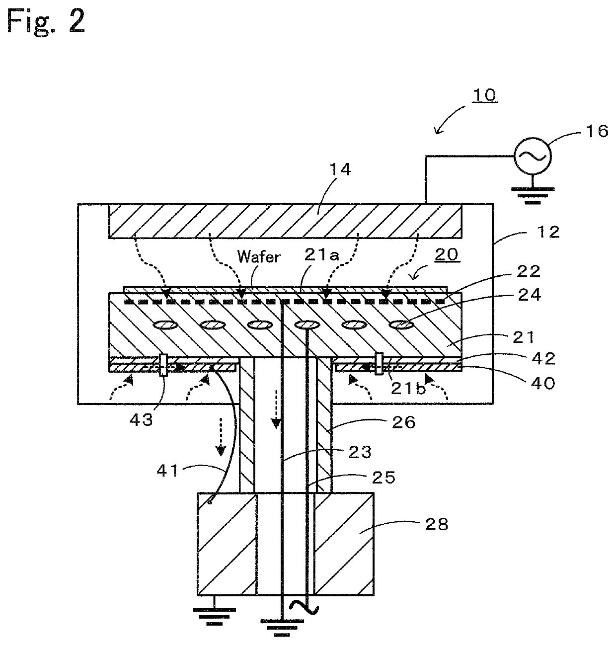
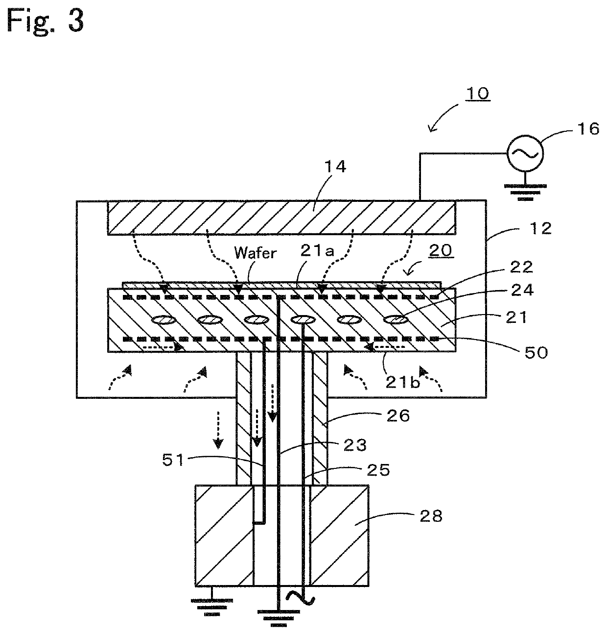
[0024]A preferred embodiment of the present invention will be described hereinafter with reference to the drawings. FIG. 1 is a longitudinal sectional view of a plasma treatment device 10. In FIG. 1, dotted-line arrows indicate plasma or plasma current.

[0025]As illustrated in FIG. 1, the plasma treatment device 10 includes a chamber 12, an upper electrode 14, and a ceramic heater 20.

[0026]The chamber 12 is a container made of an aluminum alloy or the like and formed into a box shape. The chamber 12 is provided with a pressure regulating valve, a vacuum pump, or the like (not illustrated) such that the inside of the chamber 12 can be adjusted to a desired pressure.

[0027]The upper electrode 14 is attached to the ceiling of the chamber 12. The upper electrode 14 is connected to an RF power supply 16 for plasma generation.

[0028]The ceramic heater 20 includes a ceramic plate 21, a cylindrical shaft 26, and a conductive film 30.

[0029]The ceramic plate 21 is a disk-shaped AIN ceramic membe...


PUM

PropertyMeasurementUnit
Distanceaaaaaaaaaa
Diameteraaaaaaaaaa
Electrical conductoraaaaaaaaaa

Abstract

A ceramic heater includes a disk-shaped ceramic plate having a wafer placement surface on a front surface thereof, the ceramic plate having a plasma electrode and a heater electrode embedded therein in this order, from closest to the wafer placement surface to farthest, in such a manner that the plasma electrode and the heater electrode are spaced apart from each other; a cylindrical shaft that supports the ceramic plate from a back surface of the ceramic plate; a plasma electrode connecting member arranged in the cylindrical shaft and connected to the plasma electrode; a heater electrode connecting member arranged in the cylindrical shaft and connected to the heater electrode; and a planar shield portion arranged on the back surface of the ceramic plate or embedded in the ceramic plate so as to be closer to the back surface than the heater electrode, the planar shield portion being connected to ground.

Description

BACKGROUND OF THE INVENTION1. Field of the Invention[0001]The present invention relates to a ceramic heater.2. Description of the Related Art[0002]In the related art, a semiconductor manufacturing process may adopt a plasma CVD process. In the plasma CVD process, a wafer is placed on a wafer placement surface of a ceramic heater. A plasma electrode and a heater electrode are embedded in a ceramic plate of the ceramic heater. An upper electrode is disposed in a space above the wafer. When a high-frequency voltage is applied between the upper electrode and the plasma electrode, plasma is generated between these electrodes, and a thin film is deposited on the wafer using the plasma. In such a ceramic heater, if a leakage current produced by the high-frequency voltage applied to the plasma electrode is transmitted to the heater electrode, there is a problem that energization to the heater electrode is not controllable. In this respect, PTL 1 proposes to provide a high-resistance insulat...

Claims


Application Information

Patent Timeline
IPC IPC(8): C23C16/458C23C16/46C23C16/50
CPCC23C16/4586H05B3/265C23C16/50C23C16/46H01L21/205H05B3/14H05B3/28H05B3/48H01L21/683C23C16/5096H05B3/283H05B1/0233
Inventor HARA, TOMOHIROUNNO, YUTAKA
Owner NGK INSULATORS LTD
Why Eureka
Try Eureka