Electronic component
- Summary
- Abstract
- Description
- Claims
- Application Information
AI Technical Summary
Benefits of technology
Problems solved by technology
Method used
Image
Examples
first embodiment
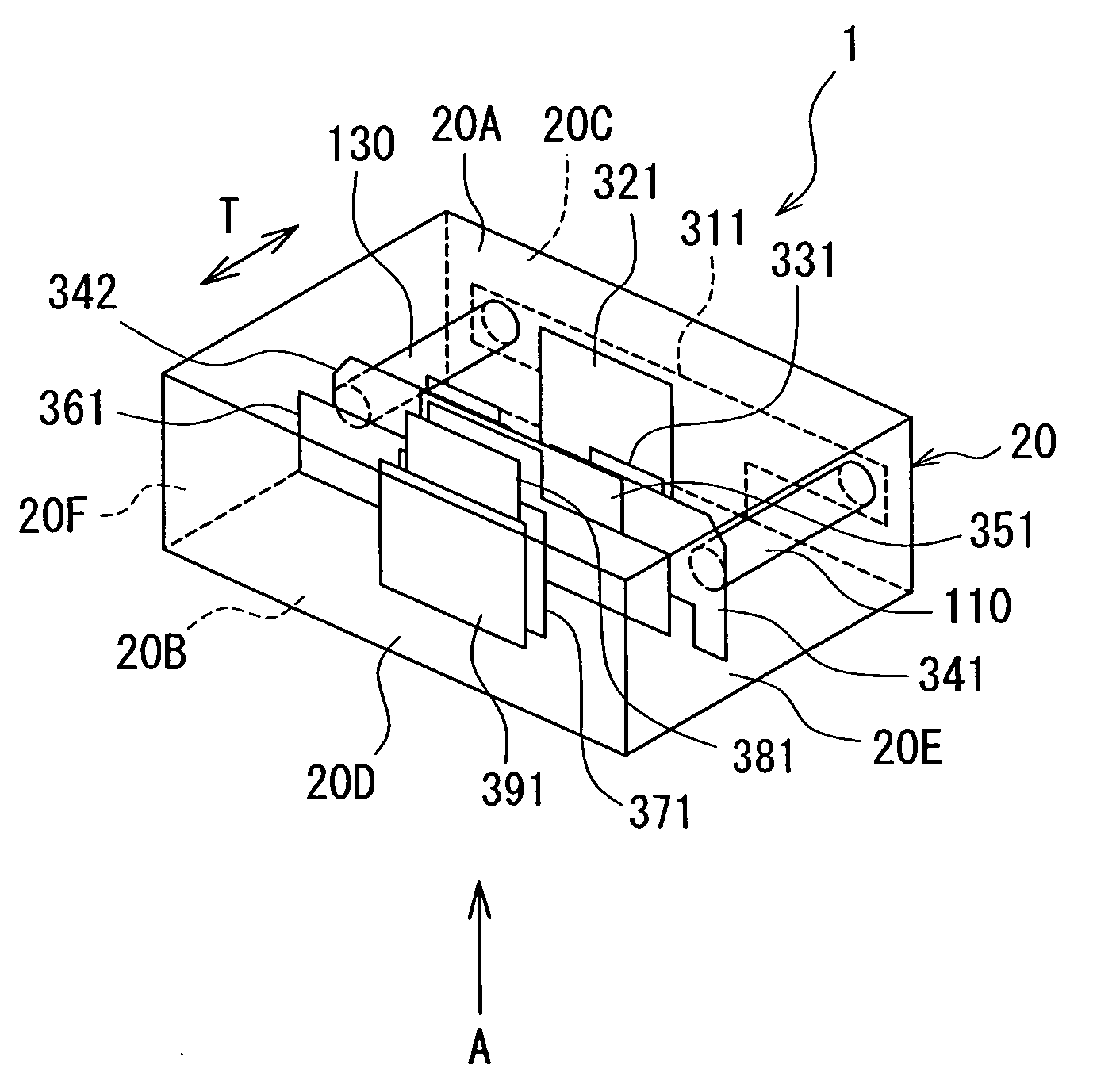
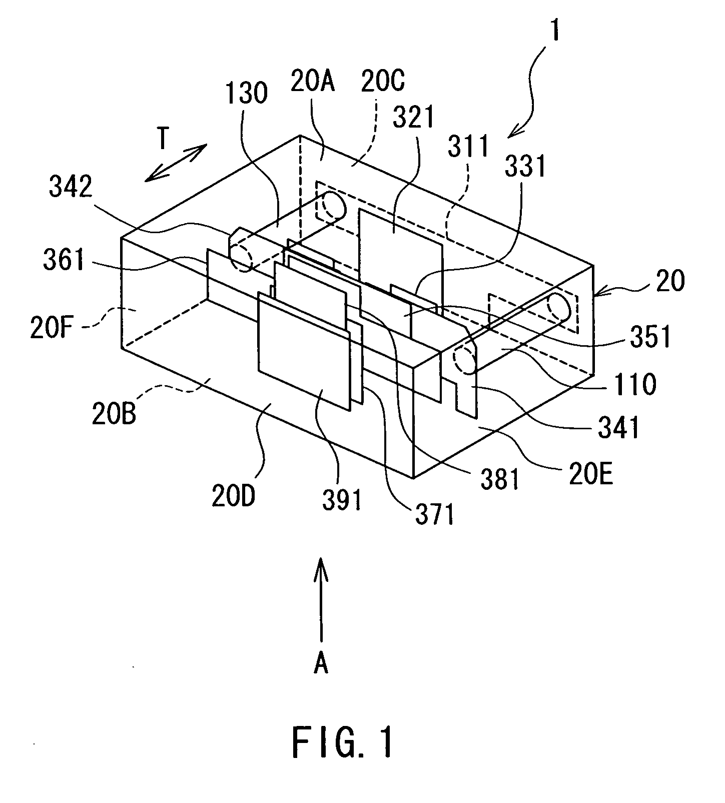
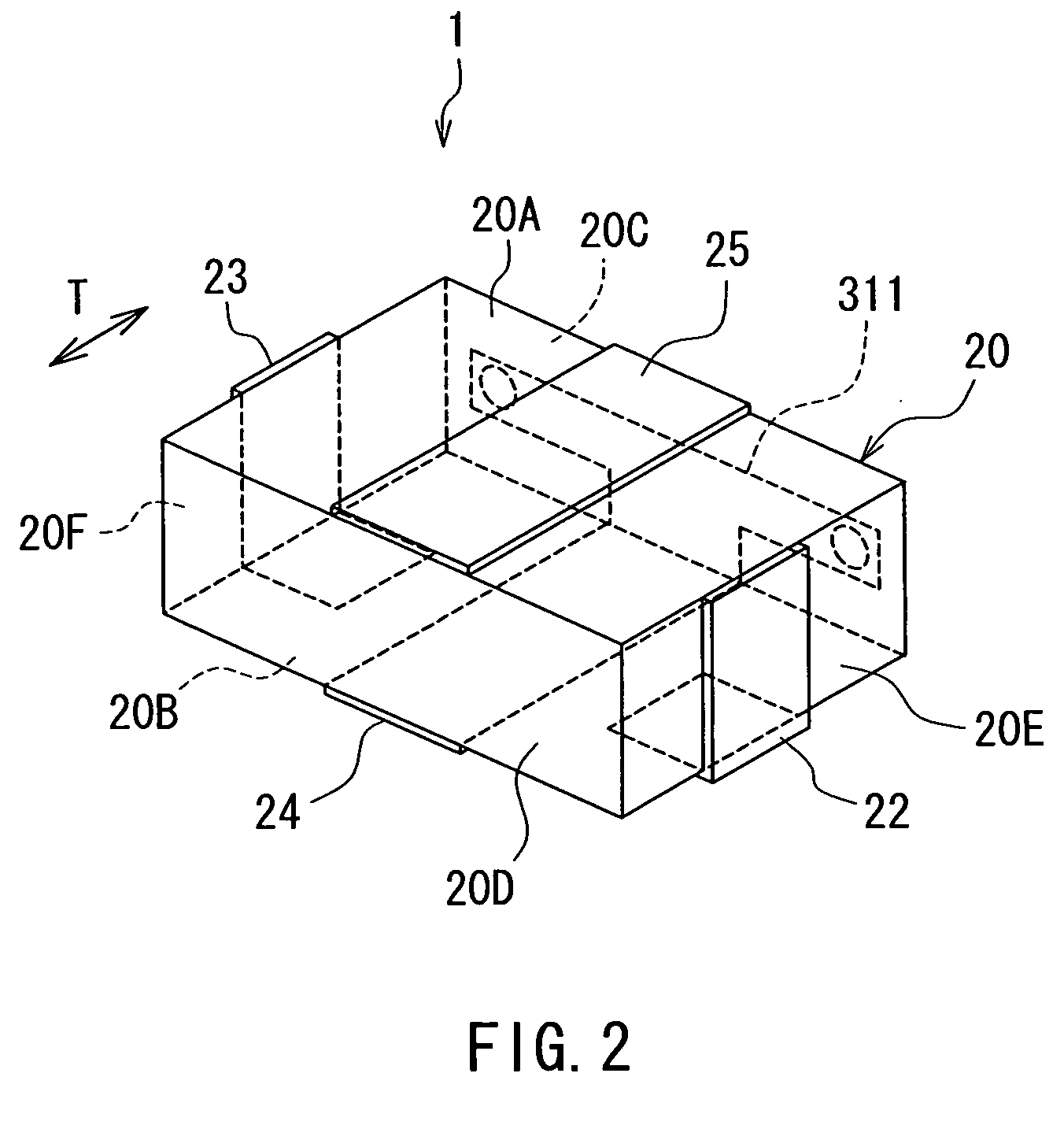
[0038]Preferred embodiments of the present invention will now be described in detail with reference to the drawings. Reference is first made to FIG. 4 to describe the circuit configuration of an electronic component of a first embodiment of the invention. The electronic component 1 of the first embodiment has the function of a bandpass filter. As shown in FIG. 4, the electronic component 1 includes an input terminal 2, an output terminal 3, three resonators 4, 5 and 6, and capacitors 17 to 19.
[0039]The resonator 4 includes an inductor 11 and a capacitor 14. The resonator 5 includes an inductor 12 and a capacitor 15. The resonator 6 includes an inductor 13 and a capacitor 16. In terms of circuit configuration, the resonator 5 is located between the resonator 4 and the resonator 6. The resonator 5 is adjacent to and inductively coupled to each of the resonators 4 and 6. The inductor 12 is inductively coupled to each of the inductors 11 and 13. In FIG. 4 the inductive coupling between ...
second embodiment
[0073]An electronic component of a second embodiment of the invention will now be described. The electronic component 1 of the second embodiment has the same circuit configuration as that of the first embodiment shown in FIG. 4.
[0074]FIG. 10 is a perspective view showing a main part of the electronic component 1 of the second embodiment. FIG. 11 is a perspective view showing the outer appearance of the electronic component 1 of the second embodiment. FIG. 12 is an illustrative view showing the main part of the electronic component 1 as viewed from direction B of FIG. 10.
[0075]The electronic component 1 includes a layered substrate 20 for integrating the components of the electronic component 1. As will be described in detail later, the layered substrate 20 includes a plurality of dielectric layers and a plurality of conductor layers that are stacked. Each of the inductors 11 and 13 is formed using two or more of the conductor layers located within the layered substrate 20. The induc...
PUM
 Abstract
Description
Claims
Application Information


