Light-emitting device, display device, imaging device, electronic device, and method for producing light-emitting device

Pending Publication Date: 2022-04-28
CANON KK
View PDF0 Cites 0 Cited by
  • Summary
  • Abstract
  • Description
  • Claims
  • Application Information

AI Technical Summary

Benefits of technology

The present invention relates to an organic light-emitting device (OLED) with improved external light reflection suppression and high luminous efficacy. The invention achieves this by employing a low-reflectance member on the light output side of the peripheral laminated section and a high-reflectance member at the first laminated section. The high-reflectance member is exposed on the substrate side for reinforcing the irradiated light wavelength components. The invention also provides a simplified process for removing the high-reflectance layer in the display region without affecting other regions, thereby ensuring the suppression of external light reflection and high luminous efficacy.

Problems solved by technology

When the external light reflection is large, reflected glare, coloration, and scattering occur and the display quality deteriorates.

Method used


Image

  • Light-emitting device, display device, imaging device, electronic device, and method for producing light-emitting device
  • Light-emitting device, display device, imaging device, electronic device, and method for producing light-emitting device
  • Light-emitting device, display device, imaging device, electronic device, and method for producing light-emitting device

Examples


first embodiment

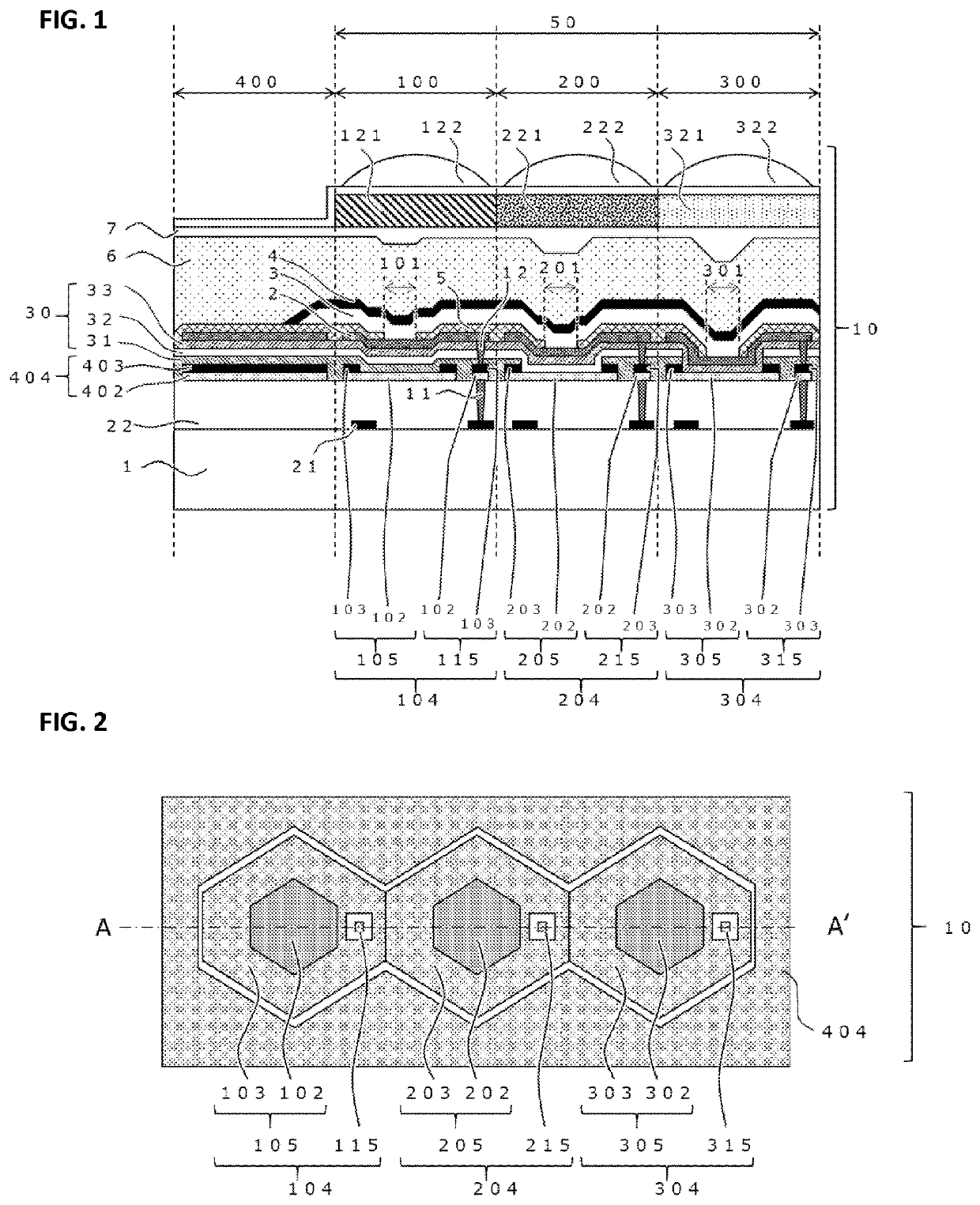
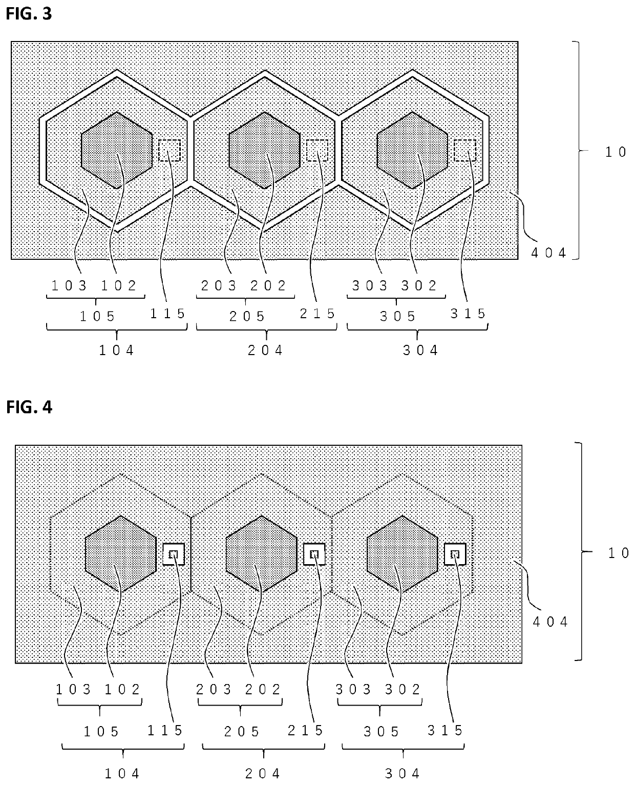
[0028]The structure of an organic EL device 10 will be described as a first embodiment of a light-emitting device according to the present invention. FIG. 1 is a schematic diagram of a cross section of the first embodiment. FIG. 2 is a schematic plan diagram of the first embodiment and shows the positional relationship in plan view of a first laminated section 104 in a display region 50 and a peripheral laminated section 404 in a peripheral region 400. FIG. 1 is a cross section along the A-A′ line segment in FIG. 2. This embodiment uses, as the light-emitting element, an organic EL light-emitting element that contains an organic light-emitting material in the light-emitting layer, but it may be constituted of a light-emitting device that uses an inorganic EL light-emitting element that contains an inorganic light-emitting material in the light-emitting layer.

[0029]In the description that follows, the upward direction refers to the direction of the light-emitting layer with respect t...

second embodiment

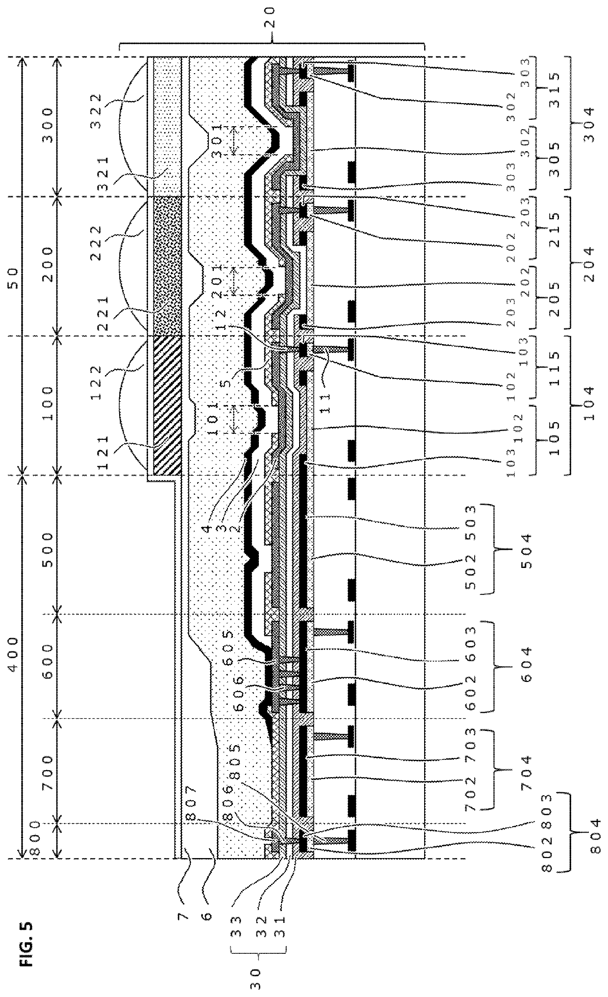
[0078]The structure of an organic EL device 20 that is provided with a plurality of organic EL devices is described as a second embodiment of the light-emitting device according to the present invention.

[0079]FIG. 5 and FIG. 6 are schematic diagrams of cross sections of the present embodiment. FIG. 7 and FIG. 8 show the relationships for the present embodiment in plan view for the first laminated section 104 of the display region 50 and the peripheral laminated section of the peripheral region 400. FIG. 5 is a schematic diagram of the cross section on the B-B′ line segment in FIG. 7, and FIG. 6 is a schematic diagram of the cross section on the C-C′ line segment in FIG. 8. In the present embodiment, the peripheral region 400 includes a dummy region 500, an upper electrode contact region 600, a wiring region 700, and a moistureproof region 800.

[0080]FIG. 5 and FIG. 7 are a structural example in which a laminated section 504 of the dummy region 500 is electrically insulated from a lam...

third embodiment

[0102]A third embodiment of the present invention will be described. In this embodiment, examples are described of the application to various devices of the light-emitting device 10 according to the first and second embodiments.

[0103]FIG. 9 is a schematic diagram that shows a display device 1000 that is an example of a display device according to the present embodiment. The display device 1000 may have, between an upper cover 1001 and a lower cover 1009, a touch panel 1003, a display panel 1005, a frame 1006, a circuit board 1007, and a battery 1008. The display panel 1005 is a display section that has a light-emitting device 10 according to the first or second embodiment, and that carries out display using light produced from the light-emitting device 10. A flexible printed circuit FPC 1002, 1004 is connected to the touch panel 1003 and the display panel 1005, respectively. A transistor-containing control circuit is printed on the circuit board 1007 and performs various types of co...


PUM


Abstract

The light-emitting device has: a display region; a peripheral region; a first light-emitting element having a light-emitting region in which a lower electrode, a light-emitting layer, and an upper electrode are laminated; a first laminated section, between the substrate and the lower electrode of the first light-emitting element, in which there are laminated a first high-reflection layer and a first low-reflection layer that has a lower reflectance than the first high-reflection layer; a peripheral laminated section, in the peripheral region, in which there are laminated on the substrate; a peripheral lamination layer in which a peripheral high-reflection layer and a peripheral low-reflection layer that has a lower reflectance than the peripheral high-reflection layer are laminated. For at least a portion of the first laminated section that overlaps in plan view with the light-emitting region, the first low-reflection layer has an opening such that the first high-reflection layer is exposed.

Description

BACKGROUND OF THE INVENTIONField of the Invention[0001]The present invention relates to light-emitting devices, display devices, imaging devices, electronic devices, and a method for producing light-emitting devices.Description of the Related Art[0002]Organic EL elements are light-emitting elements that have a pair of electrodes and, located therebetween, an organic compound layer that contains a light-emitting layer. Organic EL elements exhibit excellent characteristics, i.e., surface emission behavior, light weight, and visibility, and due to this their practical utilization as light-emitting devices, e.g., thin displays, lighting fixtures, head-mounted displays, and light sources for the print heads of electrophotographic printers, is moving forward.[0003]The demand to achieve higher definition organic EL display devices is increasing in particular. A method using a white organic EL element and color filters (the white+CF method) is known as one technology for providing higher de...

Claims


Application Information

Patent Timeline
IPC IPC(8): H01L51/52H01L51/56
CPCH01L51/5271H01L51/56H01L51/5253H10K59/352H10K59/353H10K50/858H10K50/86H10K59/88H10K59/35H10K59/38H10K50/852H10K50/856H10K50/865H10K2102/3026H10K2102/351H10K59/65H10K59/131H10K50/813H10K50/841H10K50/844H10K71/00
Inventor ISHIZUYA, KOJISANO, HIROAKI
Owner CANON KK
Why Eureka
Try Eureka