Material for organic electroluminescent element and organic electroluminescent element using the same

Active Publication Date: 2016-06-30
NIPPON STEEL CHEMICAL CO LTD
View PDF6 Cites 11 Cited by
  • Summary
  • Abstract
  • Description
  • Claims
  • Application Information

AI Technical Summary

Benefits of technology

[0032]A material for a phosphorescent device of the present invention has a structure in which at least one dibenzofuranyl group is bonded onto a carborane skeleton. A carborane compound having such structural feature enables high-level control of the electron-injecting/transporting properties because its lowest unoccupied molecular orbital (LUMO) that affects the electron-injecting/transporting properties is widely distributed in the entirety of a molecule thereof. Further, the compound enables efficient light emission from a dopant because that its triplet excitation

Problems solved by technology

Further, investigations have been made on using a europium complex as an attempt to use a triplet state, but highly efficient light emission has not been accomplished.
Thus, excessively delivered holes flow out into an electro

Method used


Image

  • Material for organic electroluminescent element and organic electroluminescent element using the same
  • Material for organic electroluminescent element and organic electroluminescent element using the same
  • Material for organic electroluminescent element and organic electroluminescent element using the same

Examples


Example

Example 1

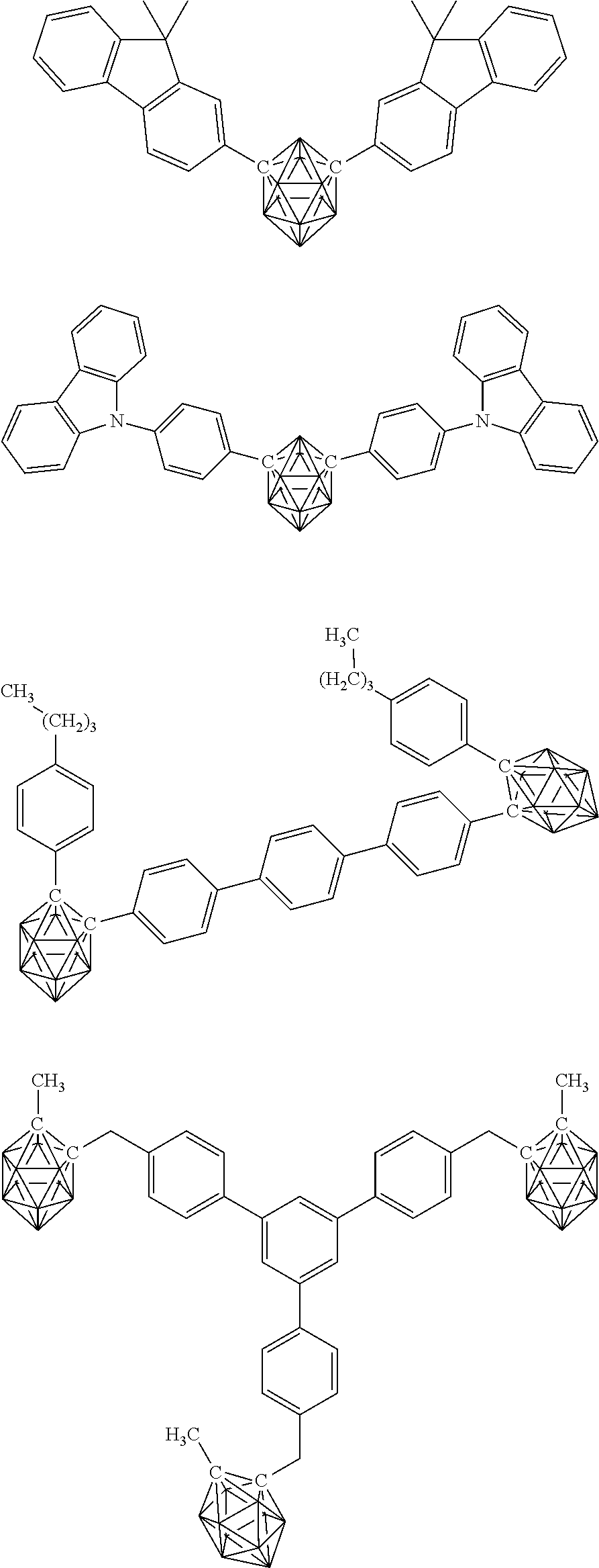
[0108]A compound 1 is synthesized in accordance with the following reaction formulae.

[0109]Under a nitrogen atmosphere, 35.0 g (0.243 mol) of m-carborane and 350 mL of 1,2-dimethoxyethane (DME) were added, and the resultant DME solution was cooled to 0° C. 96.8 mL of a 2.69 M solution of n-butyllithium in hexane was dropped to the solution, and the mixture was stirred under ice cooling for 30 minutes. 67 mL of pyridine was added to the resultant and the mixture was stirred at room temperature for 10 minutes. After that, 75.6 g (0.763 mol) of copper(I) chloride was added to the resultant and the mixture was stirred at 65° C. for 30 minutes. After that, 76.4 g (0.260 mol) of 2-iododibenzofuran was added to the resultant and the mixture was stirred at 95° C. overnight. The reaction solution was cooled to room temperature, and then the precipitated crystal was taken by filtration and the solvent was distilled off under reduced pressure. The resultant residue was purified by sil...

Example

Example 2

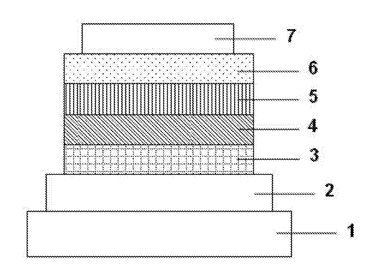
[0113]Each thin film was laminated by a vacuum deposition method at a degree of vacuum of 2.0×10⁻⁵ Pa on a glass substrate on which an anode formed of indium tin oxide (ITO) having a thickness of 70 nm had been formed. First, copper phthalocyanine (CuPC) was formed into a layer having a thickness of 30 nm to serve as a hole-injecting layer on the ITO. Next, diphenyl naphthyl diamine (NPD) was formed into a layer having a thickness of 15 nm to serve as a hole-transporting layer. Next, the compound 1 serving as a host material for a light-emitting layer and an iridium complex [iridium(III) bis(4, 6-di-fluorophenyl)-pyridinato-N,C2′]picolinate] (FIrpic) serving as a blue phosphorescent material as a dopant were co-deposited from different deposition sources onto the hole-transporting layer to form a light-emitting layer having a thickness of 30 nm. The concentration of FIrpic was 20%. Next, Alga was formed into a layer having a thickness of 25 nm to serve as an electron-transp...

Example

Examples 3 to 7

[0115]Organic EL devices were each produced in the same manner as in Example 2 except that the compound 13, 25, 26, 29, or 36 was used instead of the compound 1 as the host material for the light-emitting layer in Example 2.


PUM


Abstract

Provided are a material for an organic EL device that improves the luminous efficacy of a device, sufficiently secures its driving stability, and has a simple construction, and an organic EL device using the material. The material for an organic EL device is formed of a carborane compound having a structure in which a dibenzofuranyl group is bonded to a carborane ring. In addition, the material for an organic EL device is preferably used in a light-emitting layer, an electron-transporting layer, or a hole-blocking layer of an organic electroluminescent device having the light-emitting layer between an anode and a cathode laminated on a substrate. Also disclosed is an organic electroluminescent device using the material for an organic EL device as a host material for a light-emitting layer containing a phosphorescent light-emitting dopant and the host material.

Description

TECHNICAL FIELD[0001]The present invention relates to an organic electroluminescent device using a carborane compound as a material for an organic electroluminescent device, and more specifically, to a thin film-type device that emits light by applying an electric field to a light-emitting layer containing an organic compound.[0002]In general, an organic electroluminescent device (hereinafter referred to as organic EL device) includes a light-emitting layer and a pair of counter electrodes interposing the light-emitting layer therebetween in its simplest structure. That is, the organic EL device uses the phenomenon that, when an electric field is applied between both the electrodes, electrons are injected from a cathode and holes are injected from an anode, and each electron and each hole recombine in the light-emitting layer to emit light.[0003]In recent years, progress has been made in developing an organic EL device using an organic thin film. In order to enhance luminous efficac...

Claims


Application Information

Patent Timeline
IPC IPC(8): H01L51/00C07F5/05C09K11/02C09K11/06
CPCH01L51/008C09K11/06H01L51/0085C07F5/05H01L51/5096H01L51/5016C09K2211/1007C09K2211/1029C09K2211/185C09K11/025C07D405/14H05B33/20C09K2211/1011C09K2211/1088C07D405/10C07D209/86C07D307/91H10K85/626H10K85/6574H10K85/322H10K85/342H10K85/6572H10K50/18H10K50/11H10K2101/10B32B2457/206
Inventor OGAWA, JUNYATADA, MASASHIUEDA, TOKIKOKAI, TAKAHIRO
Owner NIPPON STEEL CHEMICAL CO LTD
Why Eureka
Try Eureka