Chip packaging method

a monolithic integrated circuit and packaging method technology, applied in the direction of electrical equipment, semiconductor devices, semiconductor/solid-state device details, etc., can solve the problems of reducing the competitive edge of the chip package structure, compromising chip performance, and complicated step of connecting the chip and the substrate with the metal wires (generally known as wire bonding), so as to improve the transmission efficiency of the resulting chip package structure, simplify the packaging process, and increase the utilization of the substrate

Active Publication Date: 2022-05-12
LINGSEN PRECISION INDS
View PDF0 Cites 0 Cited by
  • Summary
  • Abstract
  • Description
  • Claims
  • Application Information

AI Technical Summary

Benefits of technology

[0006]It can be known from the above that the chip packaging method of the present invention uses the electrically conductive metal layer instead of metal wires to electrically connect the chip and the substrate. Consequently, the various problems caused by the conventional wire bonding method are solved, the packaging process simplified, and the transmission efficiency of the resulting chip package structure enhanced.
[0007]Preferably, the substrate is used on both sides to increase substrate utilization. That is to say, the foregoing steps can be used to provide each of the top side and the bottom side of the substrate with at least one chip, a layer of encapsulant, at least one first through hole, and the corresponding electrically conductive metal plating, before the substrate is cut through the middle to form an upper part and a lower part. The upper part and the lower part are then severed according to the number of chips to produce a plurality of chip package structures. This two-sided approach can make the packaging process more efficient.
[0008]Preferably, the first through hole extends through the encapsulant and the substrate, the substrate is drilled from its bottom side and therefore has a second through hole adjacent to the chip, and the hole wall of the second through hole is plated with the electrically conductive metal along with an area that extends between the bottom side of the substrate and the bottom end of the first through hole and an area that extends between the bottom side of the substrate and the bottom end of the second through hole, so that the resulting chip package structure need not be rotated vertically by 180 degrees in order to be electrically connected to a printed circuit board. This alternative configuration increases the convenience of use of the chip package structure.

Problems solved by technology

Connecting the chip and the substrate with the metal wires (generally known as wire bonding) is a relatively complicated step of the packaging process.
Moreover, the lengths of the metal wires not only lead to relatively long transmission paths and thus compromise chip performance, but also may hinder the resulting chip package structure from meeting its dimensional requirements and thus reduce the competitive edge of the chip package structure when it comes to application to an end product.

Method used


Image

  • Chip packaging method
  • Chip packaging method
  • Chip packaging method

Examples


first embodiment

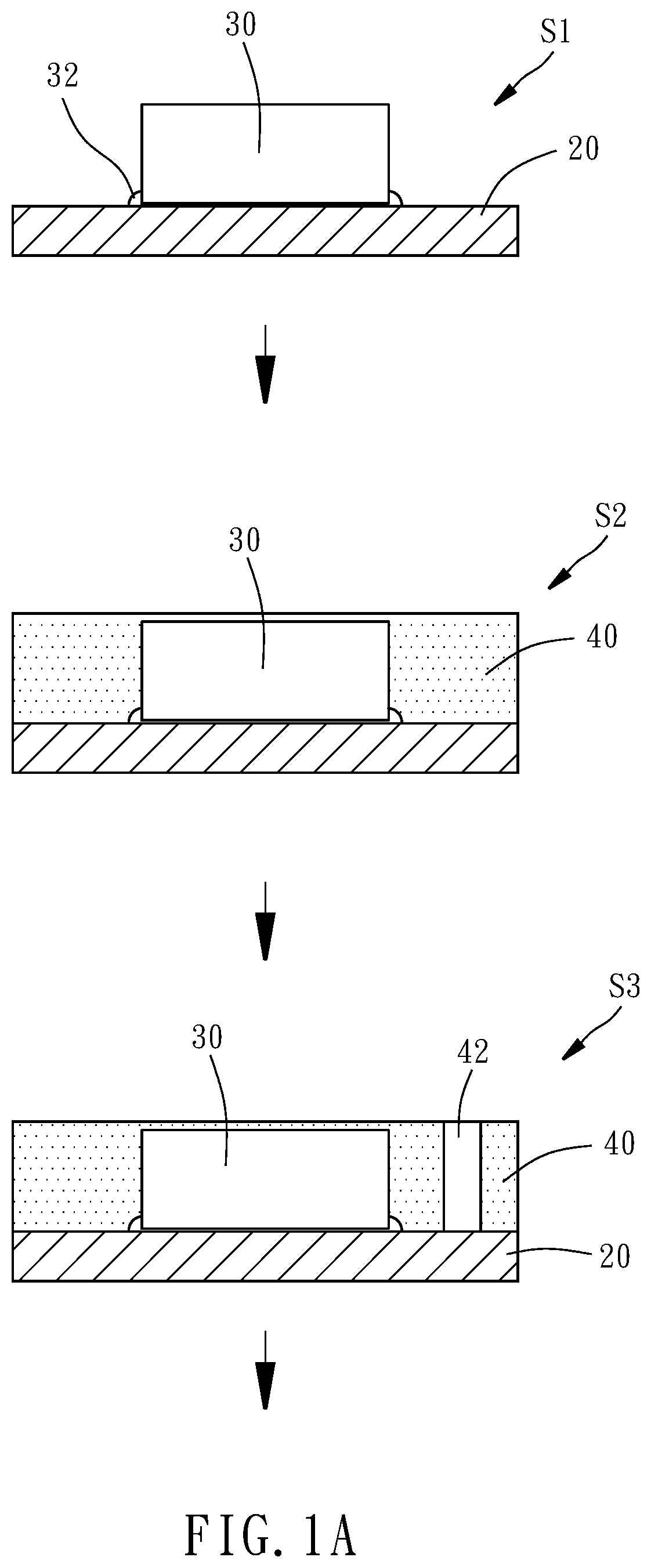
[0014]Referring to FIG. 1A and FIG. 1B, the chip packaging method according to the present invention includes the following steps:

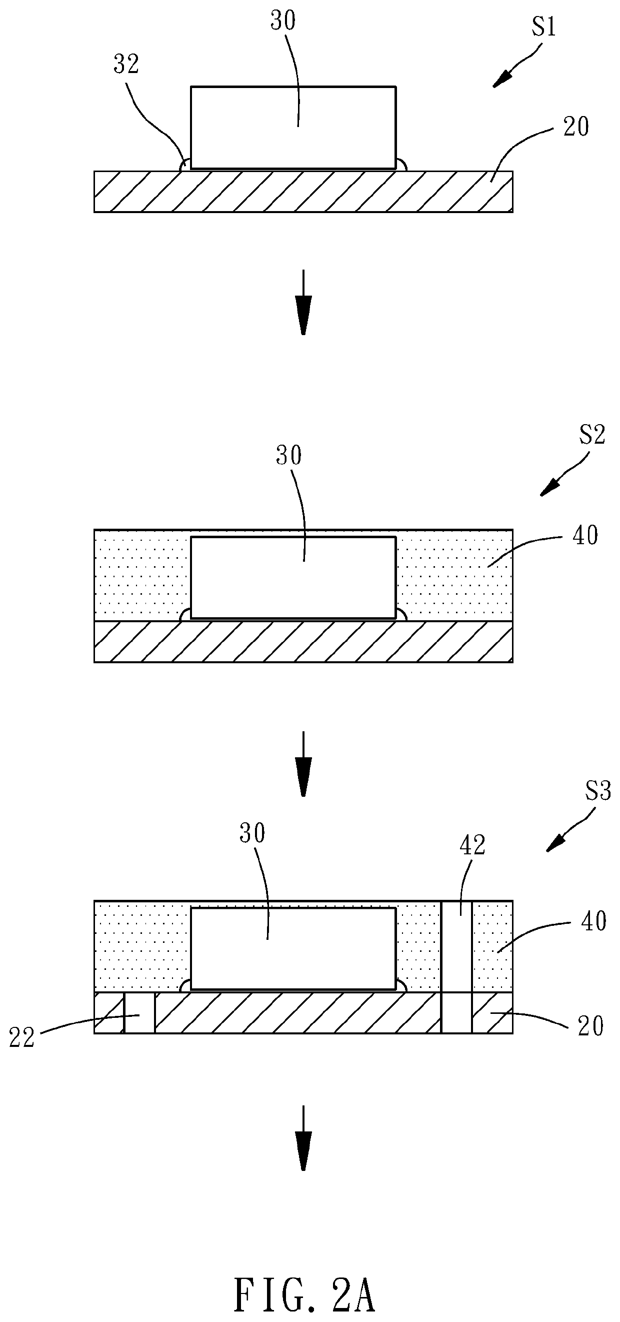
[0015]a) As indicated as step S1 in FIG. 1A, a chip 30 is fixed on the top side of a substrate 20 via an adhesive 32. The substrate 20 functions as a bridge between the chip 30 and a printed circuit board (not shown) and provides heat dissipation as well as circuit protection.

[0016]b) As indicated as step S2 in FIG. 1A, the chip 30 is encapsulated in, and thus protected by, a layer of encapsul ant 40 (e.g., epoxy resin).

[0017]c) As indicated as step S3 in FIG. 1A, a hole is drilled downward into the encapsulant 40 from the top side of the encapsulant 40 such that the encapsulant 40 has a first through hole 42 adjacent to the chip 30. The first through hole 42 extends through the top side and the bottom side of the encapsulant 40.

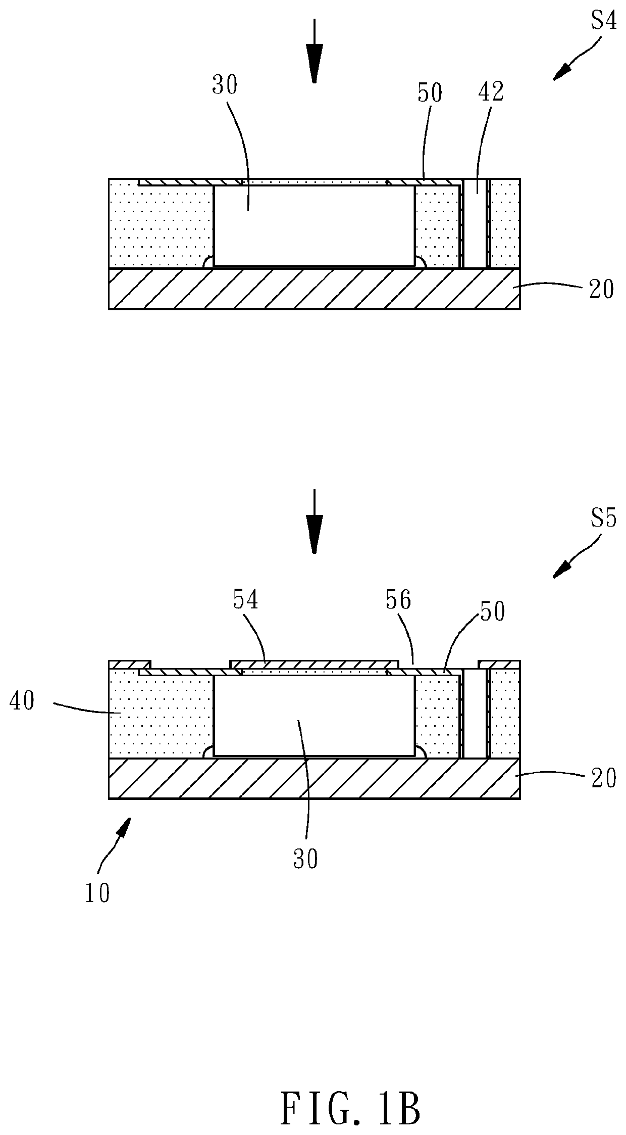
[0018]d) As indicated as step S4 in FIG. 1B, the hole wall of the first through hole 42 as well as an area extending between the...

second embodiment

[0027]According to the above, the chip packaging method according to the present invention allows the resulting chip package structure 60 to be electrically connected to a printed circuit board (not shown) through the exposed portion of the electrically conductive metal 50 on the bottom side of the substrate 20, without having to be rotated vertically by 180 degrees. The chip package structure 60, therefore, features greater convenience of use.

[0028]FIG. 3A to FIG. 3C shows the chip packaging method according to the third embodiment of the present invention. The third embodiment is generally the same as the first embodiment, the main difference being that unlike the first embodiment, whose packaging process is performed on only one side of the substrate 24, the third embodiment carries out the chip packaging method of the first embodiment on two sides of the substrate 24 at the same time to increase the utilization of the substrate 24 and the efficiency of the packaging process. Mor...

third embodiment

[0035]According to the above, the chip packaging method according to the present invention not only increases the utilization of the substrate 24, but also can produce multiple chip package structures 10 in one go to make the packaging process highly efficient.


PUM

PropertyMeasurementUnit
electrically conductiveaaaaaaaaaa
transmission efficiencyaaaaaaaaaa
lengthsaaaaaaaaaa

Abstract

A chip packaging method begins by fixing a chip to the top side of a substrate. The chip is then encapsulated in an encapsulant. After that, the encapsulant is drilled from its top side in order to have a through hole adjacent to the chip. Lastly, an area extending between the chip and the through hole and the hole wall of the through hole are plated with an electrically conductive metal to enable electrical connection between the chip and the substrate through the electrically conductive metal. The chip packaging method solves the problems of the conventional wire bonding method, simplifies the packaging process, and provides the packaged chips with high transmission efficiency.

Description

BACKGROUND OF TILE INVENTION1. Field of the Invention[0001]The present invention relates to a method for packaging a monolithic integrated circuit, or chip. More particularly, the invention relates to a chip packaging method that can simplify the packaging process and enhance the transmission efficiency of the packaged chips.2. Description of the Related Art[0002]A conventional chip packaging process typically involves fixing a chip adhesively to a substrate, connecting the chip and the substrate with a plurality of metal wires to establish an electrical connection between the chip and the substrate, and then encapsulating the chip in an encapsulant (e.g., epoxy resin) to complete the packaging process.[0003]Connecting the chip and the substrate with the metal wires (generally known as wire bonding) is a relatively complicated step of the packaging process. Moreover, the lengths of the metal wires not only lead to relatively long transmission paths and thus compromise chip performan...

Claims


Application Information

Patent Timeline
Patent Type & Authority Applications(United States)
IPC IPC(8): H01L21/56H01L21/768
CPCH01L21/56H01L2021/6027H01L21/76802H01L24/82H01L2224/92244H01L2224/8203H01L2224/24105H01L2224/32225H01L2224/24226H01L21/486H01L2224/95H01L2224/96H01L24/83H01L24/24H01L23/3121H01L23/5389H01L2224/83H01L2224/82
Inventor TU, MING-TE
Owner LINGSEN PRECISION INDS
Why Eureka
Try Eureka