
Eureka
For R&D, Eureka makes reading and utilizing patents & technical documents easy.
Eureka AIR
Designed for self-driven R&D workflows. Generate viable solutions, solve complex R&D challenges, empower your innovation with AI.

Eureka Materials
Designed for material experts only. Revolutionize your material R&D, from search, analyze, to developing new materials.

TechResearch
Generate reliable direction feasibility study reports for your R&D in just a few steps.

TechSeek
Discover and master advanced knowledge NOW. Basics, ideas, possibilities, all at once.

TechMind
As an expert in R&D Theories, TechMind can generates customized viable solutions instantly.

TechRisk
Analyze your overall solution with one click, know your potential R&D risks in advance.

TechMonitor
Get weekly tech updates, stay abreast of the latest tech innovations and key insights.
Wafer manufacturing method and laminated device chip manufacturing method
- Summary
- Abstract
- Description
- Claims
- Application Information
AI Technical Summary
Benefits of technology
Problems solved by technology
Method used
Image

Examples
first embodiment
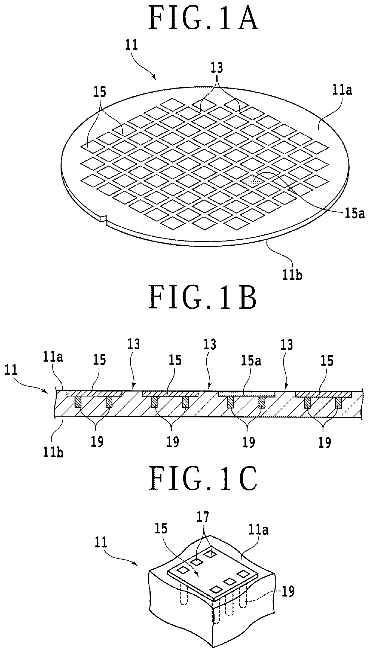
[0091]An embodiment of the present invention will hereinafter be described with reference to the accompanying drawings. An example of configuration of a wafer that can be used in the present embodiment will first be described. FIG. 1A is a perspective view depicting a wafer 11. FIG. 1B is a sectional view depicting the wafer 11.
[0092]The wafer 11 is, for example, a silicon wafer formed in a disk shape. The wafer 11 has a top surface (first surface) 11a and an undersurface (second surface) 11b on an opposite side of the top surface 11a. The top surface 11a and the undersurface 11b are formed substantially in parallel with each other.
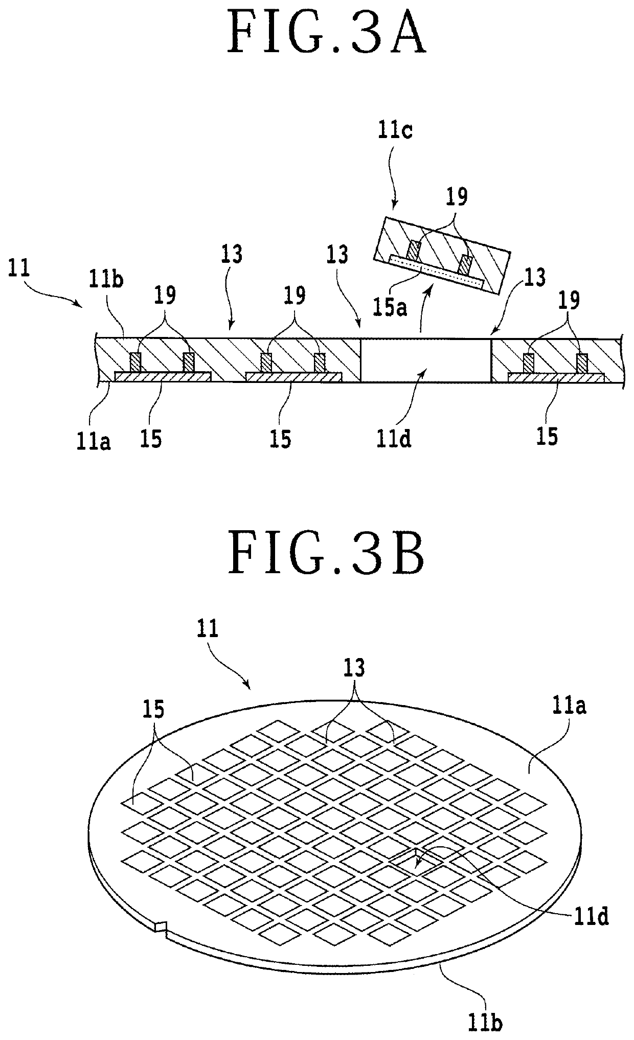
[0093]The wafer 11 is demarcated into a plurality of rectangular regions by a plurality of streets (planned dividing lines) 13 arranged in a lattice manner so as to intersect each other. Then, a semiconductor device 15 such as an integrated circuit (IC), large scale integration (LSI), a light emitting diode (LED), or microelectromechanical systems (MEMS) ...
second embodiment
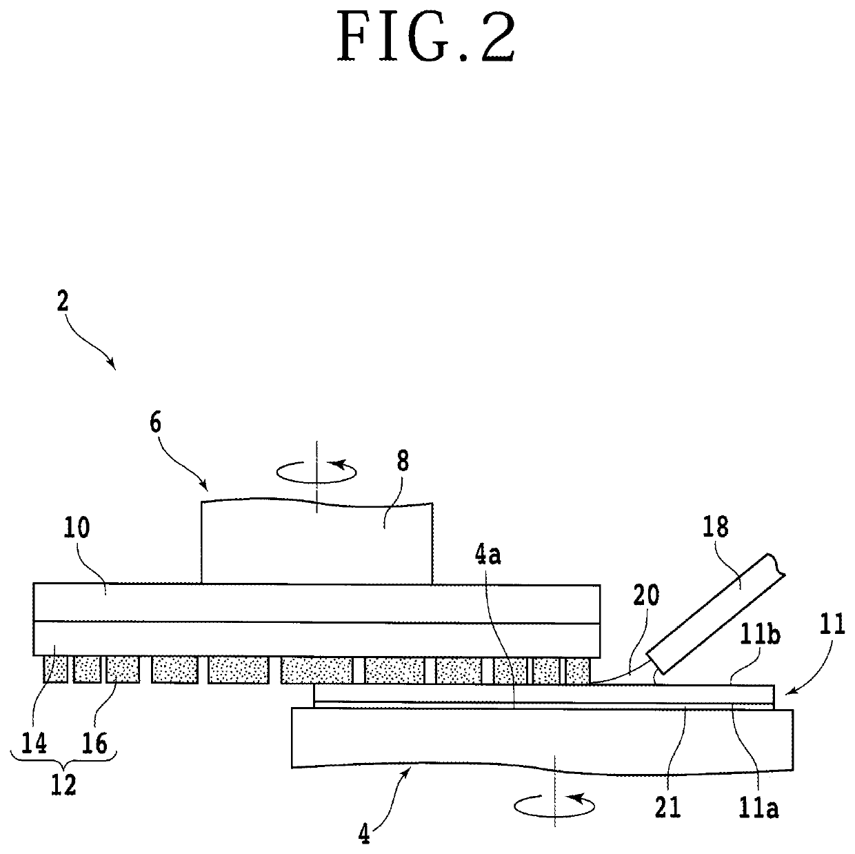
[0256]In the first embodiment, description has been made of an example in which the defective device region 11c is separated by the application of a laser beam in the removing step. However, another method may be used to separate the defective device region 11c. In the present embodiment, description will be made of a method of separating the defective device region 11c by crushing processing of crushing the wafer 11 in the removing step after performing the wafer preparing step and the grinding step (see FIG. 2).
[0257]The crushing processing used in the present embodiment is not limited as long as the crushing processing can process the wafer 11. Examples of the crushing processing that can be used to process the wafer 11 include sandblast processing, water jet processing, drill processing, and the like.
[0258]FIG. 22A is a sectional view depicting the wafer 11 in which a groove 93 is formed by the sandblast processing. A sandblast unit 72 that jets a polishing material 74 is used f...
third embodiment
[0291]In the first embodiment and the second embodiment, description has been made of an example in which the defective device region 11c is separated from the wafer 11 by processing the wafer 11 along the streets 13 in the removing step. However, a method of removing the defective device region 11c from the wafer 11 is not limited. In the present embodiment, description will be made of a method of destroying and removing the defective device region 11c by the application of a laser beam in the removing step after performing the wafer preparing step and the grinding step (see FIG. 2).
[0292]FIG. 28A is a sectional view depicting the wafer 11 irradiated with a laser beam 32D. A laser irradiating unit 30D that irradiates the wafer 11 with the laser beam 32D is used in a case where the defective device region 11c is destroyed by the application of the laser beam. Incidentally, the configuration of the laser irradiating unit 30D is similar to that of the laser irradiating unit 30A (see F...
PUM
| Property | Measurement | Unit |
|---|---|---|
| Thickness | aaaaa | aaaaa |
| Wavelength | aaaaa | aaaaa |
Abstract
Description
Claims
Application Information
 - R&D Engineer
- R&D Manager
- IP Professional
- Industry Leading Data Capabilities
- Powerful AI technology
- Patent DNA Extraction
Browse by: Latest US Patents, China's latest patents, Technical Efficacy Thesaurus, Application Domain, Technology Topic, Popular Technical Reports.
© 2024 PatSnap. All rights reserved.Legal|Privacy policy|Modern Slavery Act Transparency Statement|Sitemap|About US| Contact US: help@patsnap.com