Rectifier circuits and corresponding methods for RFID devices

a rectifier circuit and rectifier technology, applied in the direction of instruments, dc-dc conversion, apparatus without intermediate ac conversion, etc., can solve the problems of significant reduction of the return link performance and the strength of the signal received by the reader device, and achieve the effect of ensuring efficient return link performance, constant impedance, and avoiding decoupling effects

Active Publication Date: 2022-05-26
NXP BV
View PDF7 Cites 0 Cited by
  • Summary
  • Abstract
  • Description
  • Claims
  • Application Information

AI Technical Summary

Benefits of technology

[0006]This aspect is based on the idea that the desired supply voltage is selectively taken from an output terminal of one of a plurality of charge pump stages coupled in a cascade-like manner. Each single charge pump stage in the cascade is connected to the antenna input (to be charged by an input signal received from an RFID antenna) such that the cascade of charge pump stages presents a constant impedance independent of which particular charge pump stage is selected for providing the supply voltage at a given time. Hence, the power supply circuit is capable of providing a desired and limited supply voltage while maintaining an essentially constant impedance. As the charge pump stages are coupled in cascade, none of the individual charge pump stages is exposed to the total supply voltage. In other words, the charge pump stages are floating. Due to the constant impedance of the circuit, decoupling effects can be avoided, and a correspondingly efficient return link performance is assured.
[0016]In other words, the charge pumps in the cascade are arranged with alternating polarity of the charge terminals relative to the antenna input terminals such that neighboring charge pump stages receive alternating phases at their respective charging terminals. Thereby, efficient charging can be achieved for input signals with high frequency.
[0018]This aspect is essentially based on the same idea as the first aspect discussed above and provides an RFID tag utilizing the rectifier circuit according to the first aspect. Hence, the supply voltage for the RFID tag processing circuit is selectively taken from an output terminal of one of a plurality of charge pump stages coupled in a cascade-like manner. Each single charge pump stage in the cascade is connected to the antenna input (to be charged by an input signal received from the RFID antenna) such that the cascade of charge pumps presents a constant impedance independent of which particular charge pump stage is selected for providing the supply voltage at a given time. Hence, the power supply circuit is capable of providing a suitable and limited supply voltage while maintaining an essentially constant input impedance. As the charge pump stages are coupled in cascade, none of the individual charge pump stages is exposed to the total supply voltage. In other words, the charge pump stages are floating. Due to the constant input impedance of the circuit, decoupling effects can be avoided, and a correspondingly efficient return link performance is assured.
[0028]In other words, the charge pump stages in the cascade are arranged with alternating polarity of the charge terminals relative to the antenna input terminals. Thereby, efficient charging can be achieved for input signals with high frequency.
[0030]This aspect is essentially based on the same idea as the first and second aspects described above and provides a corresponding method of providing a supply voltage to an RFID tag according to which the supply voltage for the RFID tag is selectively taken from an output terminal of one of a plurality of charge pump stages coupled in a cascade-like manner. Each single charge pump stage in the cascade is connected to the antenna input (to be charged by an input signal received from the RFID antenna) such that the cascade of charge pump stages presents a constant impedance independent of which particular charge pump stage is selected for providing the supply voltage at a given time. Hence, a suitable and limited supply voltage can be provided while maintaining an essentially constant impedance. As the charge pump stages are coupled in cascade, none of the individual charge pump stages is exposed to the total supply voltage. In other words, the charge pump stages are floating. Due to the constant input impedance of the circuit, decoupling effects can be avoided, and a correspondingly efficient return link performance is assured.

Problems solved by technology

However, this approach causes the tag impedance to change and thus has a strong de-tuning effect which may lead to significant reductions in the return link performance, i.e. a reduced strength of the signal received by the reader device.

Method used


Image

  • Rectifier circuits and corresponding methods for RFID devices
  • Rectifier circuits and corresponding methods for RFID devices

Examples


Embodiment Construction

[0042]The illustration in the drawing is schematic. It is noted that in different figures, similar or identical elements are provided with the same reference signs or with reference signs, which differ only within the first digit.

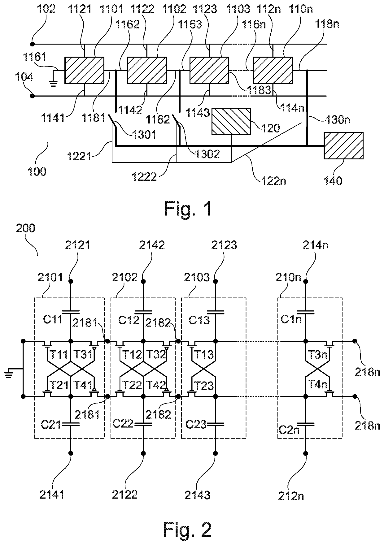
[0043]FIG. 1 shows a block diagram of a rectifier circuit 100 for an RFID tag according to an embodiment. The rectifier circuit 100 comprises a pair of antenna input terminals 102, 104 configured to receive an input signal from an RFID tag antenna (not shown), a plurality of charge pump stages 1101, 1102, 1103, 110n coupled in cascade, and a control logic 120.

[0044]Each of the charge pump stages 1101, 1102, 1103, 110n comprises a pair of charging terminals connected to the pair of antenna input terminals 102, 104, an input terminal, and an output terminal. More specifically, charge pump stage 1101 comprises charging terminal 1121 connected to antenna input terminal 102, charging terminal 1141 connected to antenna input terminal 104, input terminal 1161, and...


PUM


Abstract

There is described a rectifier circuit for providing and limiting a supply voltage to an RFID tag, the circuit including a pair of antenna input terminals configured to receive an input signal from an RFID tag antenna. A plurality of charge pump stages are coupled in cascade in such a way that an input terminal of a first charge pump stage in the cascade is connected to ground and an input terminal of each subsequent charge pump stage in the cascade is coupled to an output terminal of the preceding charge pump stage in the cascade. A control logic is configured to select the output terminal of one charge pump stage among the plurality of charge pump stages to provide the supply voltage. Furthermore, an RFID tag and a method of providing and limiting a supply voltage to an RFID tag are described.

Description

TECHNICAL FIELD[0001]The present disclosure relates to the field of RF communication devices. More specifically, the present disclosure relates to rectifier circuits and methods for providing and limiting a supply voltage to an RFID tag. Furthermore, the present disclosure relates to an RFID tag comprising a corresponding rectifier circuit.ART BACKGROUND[0002]State of the art passive UHF RFID tags use a charge pump for generating the main power supply, i.e. by converting the AC voltage from the antenna into a DC supply voltage. The output voltage of this rectifier is strongly dependent on input power and impedance matching. To prevent physical damage to the electronic components in RFID tags, state of the art implementations utilize a charge pump limiter that clamps the output voltage of the rectifier to a certain level. However, this approach causes the tag impedance to change and thus has a strong de-tuning effect which may lead to significant reductions in the return link perform...

Claims


Application Information

Patent Timeline
Patent Type & Authority Applications(United States)
IPC IPC(8): G06K19/07G06K19/077H02M3/07
CPCG06K19/0713H02M3/075G06K19/07773G06K19/0723H02M3/07H02M7/04
Inventor PICHLER, THOMASREBOLLO PIMENTEL, IVAN JESUS
Owner NXP BV
Why Eureka
Try Eureka