Eureka AIR delivers breakthrough ideas for toughest innovation challenges, trusted by R&D personnel around the world.

Micro LED adsorption body

Pending Publication Date: 2022-05-26
POINT ENG
View PDF0 Cites 0 Cited by
  • Summary
  • Abstract
  • Description
  • Claims
  • Application Information

AI Technical Summary

Benefits of technology

The present invention provides a micro LED adsorption body with a buffer part to prevent damage to the micro LEDs during adsorption. This results in a higher transfer efficiency and reduces the occurrence of micro LED damage.

Problems solved by technology

In particular, in relation to the transfer of the micro LED device to the display substrate, as the micro LED size is reduced to 1 μm to 100 μm, conventional pick-and-place equipment may not be used, and a transfer head technology for higher precision transfer is required.
This method may cause a problem with respect to damage to the micro LEDs caused by the charging phenomenon due to voltage applied to the electrostatic head during electrostatic induction.
In this method, there is no problem of damage to the micro LEDs compared to the electrostatic head method, but there are disadvantages in that the micro LEDs may be stably transferred only when adhesive strength of an elastic transfer head is greater than that of a target substrate in a transfer process, and an additional process for electrode formation is required.
However, Related Art 3 has a disadvantage in that it is difficult to produce an adhesive structure of cilia.
However, Related Art 4 requires continuous use of the adhesive, and has a disadvantage in that the micro LEDs may be damaged when the roller is pressed.
Samsung Display Co., Ltd proposed a method of transferring micro LEDs to an array substrate by means of electrostatic induction by applying a negative voltage to first and second electrodes of the array substrate in a state where the array substrate is immersed in a solution (Korean Patent Application Publication No. 10-2017-0026959, hereinafter referred to as “Related Art 5”) However, Related Art 5 has a disadvantage in that a separate solution is required so that the micro LEDs are immersed in the solution and transferred to the array substrate, and a subsequent drying process is required.
However, since Related Art 6 is a method of transferring the micro LEDs to adhesive surfaces of the plurality of pickup heads by applying a bonding material having adhesive strength, there is a disadvantage in that a separate process of applying the bonding material to the pickup heads is required.
However, since these disadvantages are derived from the basic principles adopted by the related inventions, there is a limit to improving the disadvantages while maintaining the basic principles.

Method used


Image

  • Micro LED adsorption body
  • Micro LED adsorption body
  • Micro LED adsorption body

Examples


Embodiment Construction

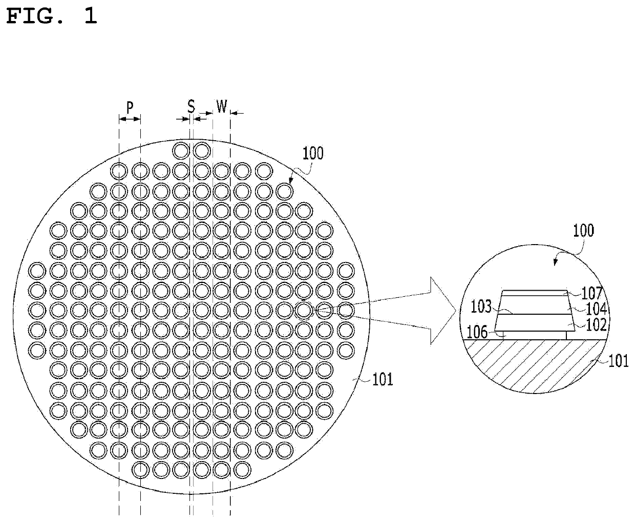
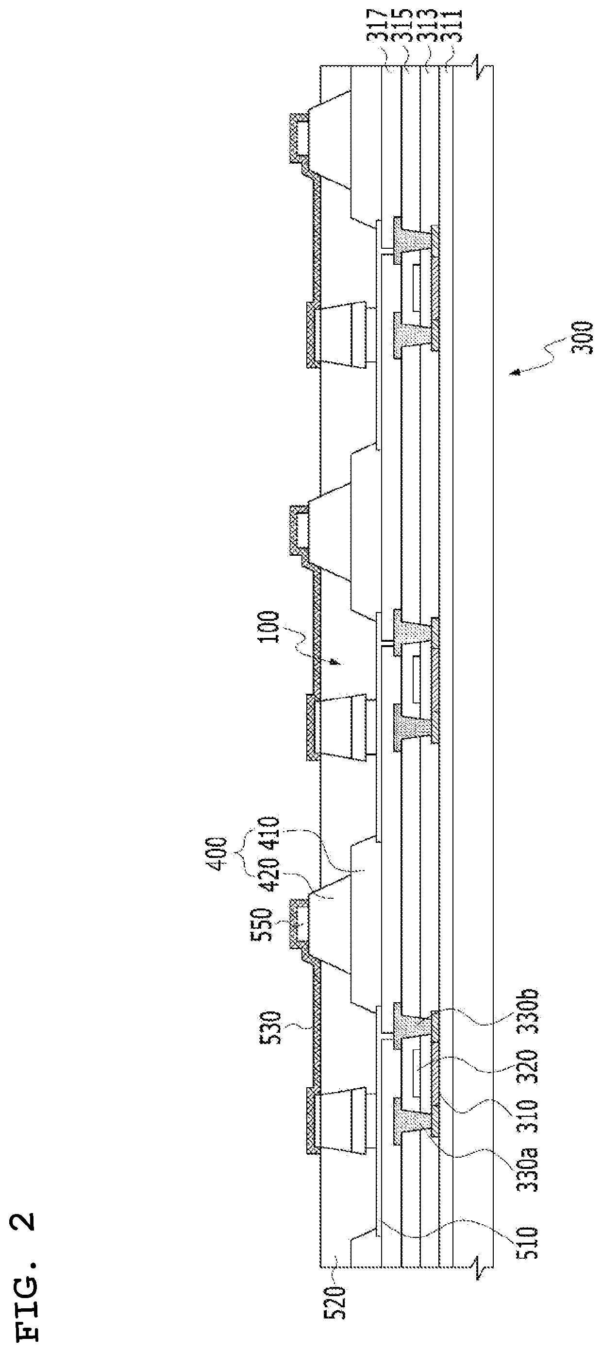
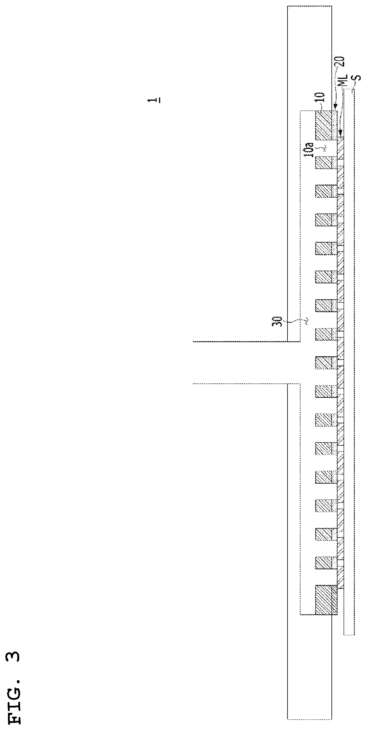
[0039]The following is merely illustrative of the principles of the invention. Therefore, although not explicitly described or shown herein, those skilled in the art can embody the principles of the invention and devise various devices that are included in the spirit and scope of the invention. In addition, it should be understood that all conditional terms and examples listed herein are, in principle, expressly intended only for the purpose of understanding the inventive concept and are not limited to the specifically enumerated exemplary embodiments and states as such.

[0040]The above-described objectives, features, and advantages will become more apparent through the following detailed description in conjunction with the accompanying drawings, and accordingly, those skilled in the art to which the present invention pertains will be able to easily implement the technical idea of the present invention.

[0041]The exemplary embodiments described herein will be described with reference ...


PUM


Abstract

A micro LED vacuum adsorption body configured to vacuum-adsorb micro LEDs is proposed. More particularly, the micro LED adsorption body is capable of preventing micro LED damage when adsorbing the micro LEDs.

Description

TECHNICAL FIELD[0001]The present invention relates to an adsorption body configured to adsorb micro LEDs.BACKGROUND ART[0002]Currently, while LCDs still dominate in the display market, OLEDs are rapidly replacing LCDs and emerging as mainstream products. In a current situation where display makers are in a rush to participate in the OLED market, micro light-emitting diode (hereinafter referred to as “micro LED”) displays have emerged as another next-generation display. Liquid crystal and organic materials are respectively the core materials of LCDs and OLEDs, whereas the micro LED display uses an LED chip itself in units of 1 to 100 micrometers (μm) as a light emitting material.[0003]Since the term “micro LED” emerged in the patent “MICRO-LED ARRAYS WITH ENHANCED LIGHT EXTRACTION” in 1999 (Korean Patent No. 10-0731673) disclosed by Cree Inc., research and development is in progress as related research papers based thereon have been published one after another. In order to apply the ...

Claims


Application Information

Patent Timeline
IPC IPC(8): H01L21/683H01L21/67
CPCH01L21/6838H01L21/67144H01L33/0095H01L25/0753H01L33/62H01L21/67712H01L21/67721
Inventor AHN, BUM MOPARK, SEUNG HOBYUN, SUNG HYUN
Owner POINT ENG
Why Eureka
Eureka Blog
Learn More