Method for fabricating a compound semiconductor epitaxial wafer

Inactive Publication Date: 2006-01-19
INST NUCLEAR ENERGY RES ROCAEC
View PDF23 Cites 6 Cited by
  • Summary
  • Abstract
  • Description
  • Claims
  • Application Information

AI Technical Summary

Benefits of technology

[0012] The method for fabricating the compound semiconductor on the silicon substrate in the present invention is as follows: Firstly, a deposition is applied on a silicon substrate to deposit an amorphous silicon film as a silicon first buffer layer. Then, a deposition for epitaxy growth at a lower temperature is applied on the silicon first buffer layer to deposit a layer of a compound semiconductor film as a compound semiconductor second buffer layer. Then, an epitaxy process for epitaxy growth at a regular temperature is applied on the compound semiconductor second buffer layer to form an epitaxy film of compound semiconductor as a compound semiconductor first epitaxy layer. Then, a heat treatment of thermal cycle annealing is directly applied to the epitaxy growth system to lower the occurrence of the threading dislocation. Then, an epitaxy process for epitaxy growth at a regular temperature is applied on the compound semiconductor second first epitaxy layer to form an epitaxy film of compound semiconductor as a compound semiconductor second epitaxy layer. And then, a heat treatment process of thermal cycle annealing is applied again to eliminate the stress between the silicon substrate and the compound semiconductor second epitaxy layer.
[0013] On comparing with the prior arts, the present invention has the following advantages:
[0014] 1. The whole epitaxy and the heat treatment are completed in the same epitaxy growth system without applying an epitaxy process again out of the original system so that the complexity of the process and the chance of being polluted are reduced.
[0015] 2. The present invention uses a silicon first buffer layer together with a compound semiconductor second buffer layer as the buffer materials between a silicon substrate and compound semiconductor epitaxy layers. By doing so, when processing the heat treatment, the occurrences of the threading dislocations can be reduced by the mutual behaviors of the silicon first buffer layer and the compound semiconductor second buffer layer so that compound semiconductor epitaxy layers with better quality can be obtained.
[0016] 3. Two times of thermal cycle annealing are applied in the present invention to have an effective use of the silicon first buffer layer and the compound semiconductor second buffer layer so that the quality of the compound semiconductor epitaxy layers can be improved.
[0017] 4. The double crystal X-ray rocking curve of the compound semiconductor epitaxy layer made according to the present invention is measured and the result shows a reduction to an FWHM of 105 arcsec (arcsecond). As comparing to the experiment result from Takano et al. as 140 arcsec, that from Itoh et al. as 130 arcsec and that from Hao et al. as 118 arcsec, the compound semiconductor epitaxy layers made by the present invention comprises epitaxy with better quality.

Problems solved by technology

But, some problems exist between the two materials of the monocrystalline silicon and the—compound semiconductor, like the lattice mismatch and the different thermal expansion coefficients.
But because the heat treatment and the epitaxy process is combined together, the complexity of the process is increased.
But, since a re-growth has to be comprised in the method, the complexity of the method is increased as well.
Besides, the epitaxial wafer is apt to be polluted and so the yield of the whole procedure is affected.

Method used


Image

  • Method for fabricating a compound semiconductor epitaxial wafer
  • Method for fabricating a compound semiconductor epitaxial wafer
  • Method for fabricating a compound semiconductor epitaxial wafer

Examples


Embodiment Construction

[0026] The following descriptions of the preferred embodiments are provided to understand the features and the structures of the present invention.

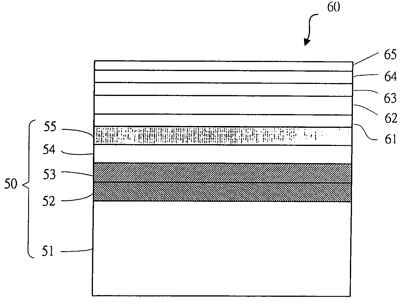
[0027]FIG. 5, FIG. 6 and FIG. 7 are views showing the fabrication method for a compound semiconductor epitaxial wafer according to the present invention. As shown in FIG. 5, a metal-organic chemical vapor deposition (MOCVD) process is applied in the present invention. Firstly, a deposition is applied on a silicon substrate 51 at 580° C. (Celsius degree) by using a process gas of SiH4 to form a layer of an amorphous silicon film with a thickness of 10-25 Å (angstrom) to be a silicon first buffer layer 52. Then, a deposition is applied on the silicon first buffer 52 layer at 300° C. by using a process gas of Ga(CH3)3 and AsH3 to form a layer of GaAs with a thickness of 100 Å to be a compound semiconductor second buffer layer 53. Then, an epitaxy process is applied on the compound semiconductor second buffer layer 53 at 710° C. by using a p...


PUM


Abstract

The present invention discloses a compound semiconductor epitaxial wafer and its fabrication method. The method comprises the steps of the followings: depositing a first buffer layer of silicon on a silicon substrate; depositing a compound semiconductor second buffer layer on the first buffer layer; growing a compound semiconductor first epitaxy layer on the second buffer layer; reducing the threading dislocation density by a thermal treatment, which is caused by the discrepancy in the lattice constants or in the thermal expansion coefficients of the silicon substrate and the compound semiconductor epitaxy layers; growing a compound semiconductor second epitaxy layer on the first epitaxy layer; and, applying a thermal treatment again. Accordingly, a compound semiconductor epitaxy layer with excellent crystal quality is obtained.

Description

FIELD OF THE INVENTION [0001] The present invention relates to a method for fabricating a compound semiconductor epitaxial wafer. More particularly, it relates to a fabrication method for a good quality crystal formed on a compound semiconductor epitaxy layer by the followings of a silicon buffer layer, a compound semiconductor buffer layer, a compound semiconductor epitaxy layer and heat treatments. DESCRIPTION OF THE RELATED ARTS [0002] The technology of photoelectricity industry and the communication industry has progressed a lot during the past years, so the role of the—compounds is becoming increasingly important. The—compounds such as GaAs, etc. have become the main base materials for photoelectrical or communicational components owing to its characteristics in direct band-gap and high carrier mobility, and its ability in obtaining materials with different band-gaps by adjusting the chemical composition of the—compounds. The photoelectrical and the communicational components o...

Claims


Application Information

Patent Timeline
IPC IPC(8): C30B23/00C30B25/00C30B28/12C30B28/14
CPCC30B29/42C30B25/18
Inventor LAN, SHAN-MINGSHIN, HWA-YUH
Owner INST NUCLEAR ENERGY RES ROCAEC
Why Eureka
Try Eureka