
Semiconductor package device

a technology of semiconductors and package devices, applied in the field of semiconductor package devices, can solve the problems of increasing power consumption, reducing yield rate, and prone to warpage of carriers b>10/b>, and achieve the effect of improving the structure of stacked packages

Active Publication Date: 2022-06-02
PHOENIX PIONEER TECH
View PDF15 Cites 0 Cited by
  • Summary
  • Abstract
  • Description
  • Claims
  • Application Information

AI Technical Summary

Benefits of technology

The object of this invention is to create a package device that combines efficient use of space, structural rigidity and a simple packaging process. It has a stacked package structure that achieves this.

Problems solved by technology

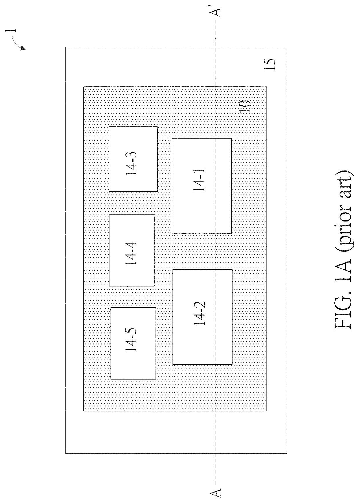
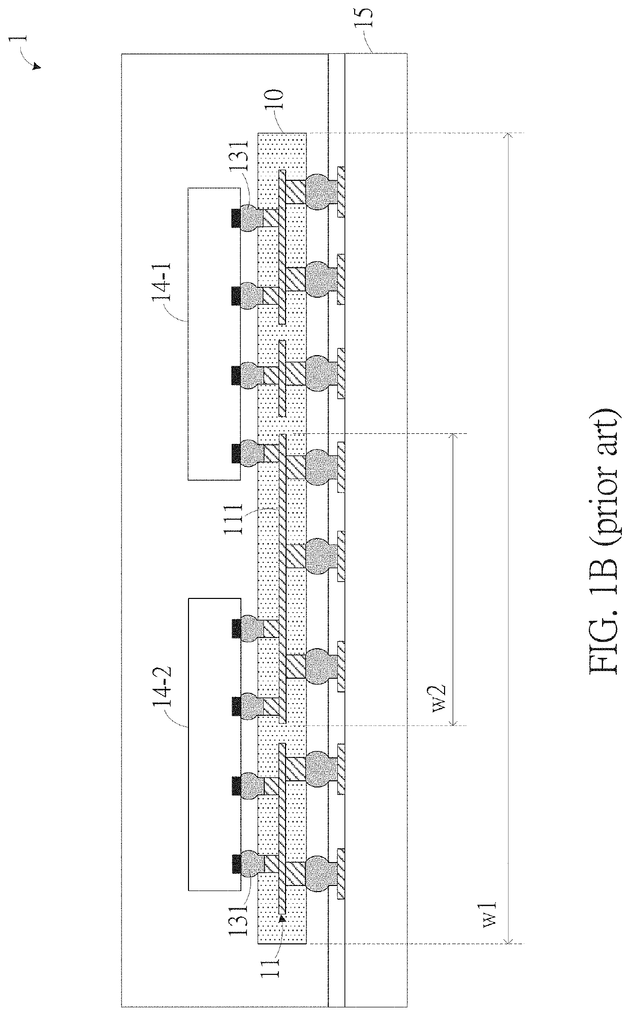
In addition, in order to transmit the signals of the chips 14-1 to 14-5 across the chip, the length of each part of the conductive layer 11 of the carrier 10 in the horizontal direction (especially the length w2 of a part 111 of the conductive layer 11) must also be increased, resulting in an increase in power consumption.
Furthermore, because more than two chips 14-1˜14-5 are carried at the same carrier, the carrier 10 is prone to warpage and the yield rate decreases.
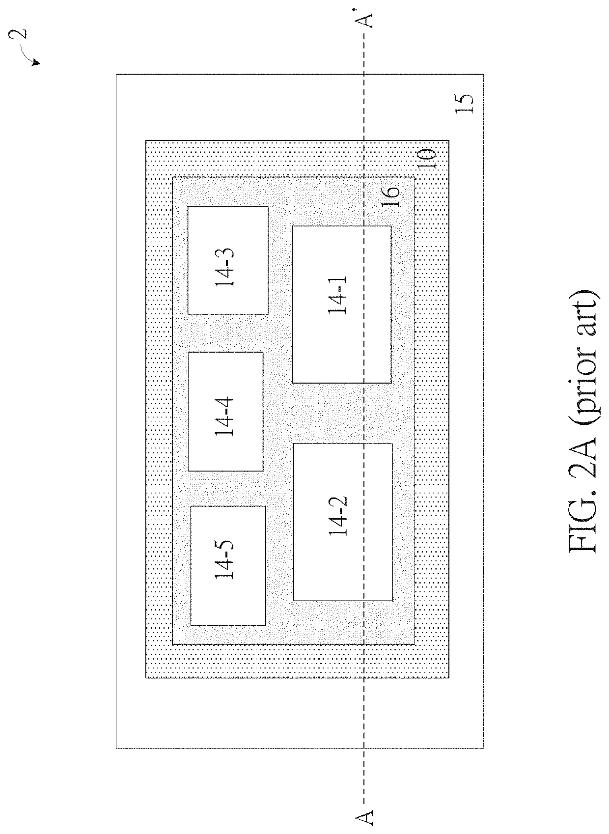
However, the additional silicon interposer 16 will result in additional material costs and packaging processes, which is a problem with the 2.5D package device 2 in the prior art.
Through the above method, the chips 14-1 to 14-3 are stacked in a vertical direction, however, the above stacked configuration will cause the chips 14-1 to 14-3 to heat dissipation difficulties and generate high temperatures.
However, the conductive pillar 137 inevitably increases the lateral area (i.e., the area in the horizontal direction) of the PoP stacked package device 3a, which is a problem of the stacked package device 3a in the prior art.

Method used


Image

  • Semiconductor package device
  • Semiconductor package device
  • Semiconductor package device

Examples


first embodiment

[0042]FIG. 5A to FIG. 5C are respectively a schematic top view and a schematic cross-sectional view of the package structure of a semiconductor package device 5 of the invention. As shown in FIG. 5A, the semiconductor package device 5 is disposed on a circuit board 45, and a flexible carrier 30, which is flexible or bendable, is to replace the rigid carrier of the prior art (for example, instead of the rigid carriers 10 and 18 shown in FIG. 3A).

[0043]As shown in FIG. 5B, the flexible carrier 30 includes a flexible layer 31 and a rigid layer 32. The flexible layer 31 has a patterned build-up circuit 311 and is flexible. The rigid layer 32 is bonded to a part of the surface of the flexible layer 31. The part where the flexible layer 31 is combined with the rigid layer 32 can be formed into a first carrying part 33 and a second carrying part 34. The flexible layer 31 without the rigid layer 32 between the first carrying part 33 and the second carrying part 34 is formed as a first flexi...

second embodiment

[0064]In addition, since the second flexible part 46 of the flexible carrier 30a can be flexed downwards, the side package part 53 and the bottom package part 51 can be arranged in an appropriate position on the same plane. In addition, the side package part 53 is electrically connected to the circuit board 45a through the solder bump 365, so that the space above the side package part 53 can accommodate other components, which greatly improves the space utilization and the flexibility of package design. In other words, the flexible carrier 30a of this embodiment has greater flexibility and space utilization in both the horizontal and vertical directions, so that the package size of the semiconductor package device 6 in both the horizontal and vertical directions can be reduced. The mentioned above are the technical effects of the invention.

[0065]As mentioned above, since there is still an idle space above the side package part 53, a fifth chip 37-5 can be further stacked on the four...


PUM

PropertyMeasurementUnit
flexibleaaaaaaaaaa
sizeaaaaaaaaaa
length w1aaaaaaaaaa

Abstract

A semiconductor package device includes a flexible carrier, a first chip, a second chip, a first molding layer, a first adhesive layer and a second molding layer. The flexible carrier has a flexible layer and a rigid layer. The flexible layer has a patterned build-up circuit. The rigid layer is connected to a portion surface of the flexible layer. The position that the flexible layer connected to the rigid layer is formed a first carrying part and a second carrying part. The region of the flexible layer between the first carrying part and the second carrying part without the rigid layer is formed as a first flexible part. The first chip is connected to the first carrying part by flip-chip manner and the second chip is connected to the second carrying part by flip-chip manner. The first molding layer covers the first chip and the second molding layer covers the second chip. The first adhesive layer is connected between the first molding layer and the second carrying part.

Description

CROSS REFERENCE TO RELATED APPLICATIONS[0001]This Non-provisional application claims priority under 35 U.S.C. § 119(a) on Patent Application No. 109142356 filed in Republic of China on Dec. 2, 2020, the entire contents of which are hereby incorporated by reference.BACKGROUND OF THE INVENTIONField of the Invention[0002]The invention relates to a package device, and particularly relates to a semiconductor package device of a system in package (SIP).Descriptions of the Related Art[0003]Science and technology are changing with each passing day, and semiconductor chips (dies) have been widely used in daily life. With the evolution of semiconductor manufacturing process and packaging technology, the size of chips has been gradually reduced, and a system composed of multiple chips or other components can be integrated into a single package, which is called system in package (SIP). In the package device of various systems integration in the prior art, there are different aspects of the pack...

Claims


Application Information

Patent Timeline
Patent Type & Authority Applications(United States)
IPC IPC(8): H01L23/538H01L23/31H01L25/10
CPCH01L23/5387H01L23/3121H01L24/16H01L23/5383H01L2224/16235H01L25/105H01L23/4985H01L23/49822H01L23/49838H01L23/3107H01L25/18H01L23/49816H01L23/5385H05K3/4691H01L2224/48227H01L2224/49175H01L2924/00014H01L2224/48091H01L2924/15192H01L2924/181H01L24/48H01L24/32H01L24/49H01L2224/05553H01L2924/15311H01L2224/16225H01L2224/48235H01L2224/73265H01L2224/73253H01L24/73H01L2224/16145H01L2224/16146H05K1/189H05K2201/10674H05K1/148H01L25/0657H01L2225/0651H01L2225/06517H01L2225/06568H01L2224/45099H01L2924/00012H01L2224/32145
Inventor YU, CHUN-HSIENHSU, SHIH-PINGTSAI, HSIEN-MING
Owner PHOENIX PIONEER TECH
Learn More