Array substrate and display panel

a technology applied in the field of array substrate and display panel, can solve problems such as uneven brightness, and achieve the effect of improving the terrain (surface unevenness) of the inverted triangle area

Pending Publication Date: 2022-06-23
SHENZHEN CHINA STAR OPTOELECTRONICS SEMICON DISPLAY TECH CO LTD
View PDF2 Cites 0 Cited by
  • Summary
  • Abstract
  • Description
  • Claims
  • Application Information

AI Technical Summary

Benefits of technology

[0033]The present application provides an array substrate and a display panel. The array substrate comprises a fan-out region arranged at one side of a display region, and is formed between two adjacent fan-out regions at a same side of the display region. In an inverted triangle region of the present application, floating metal lines are arranged at a non-wiring portion of the inverted triangle region, that is, the floating metal line is arranged between the first metal line and the second metal lines to improve a terrain (surface unevenness) of the inverted triangle area. Thereby, a “retaining wall” effect caused by the second metal line in the inverted triangle region is weakened, and consequently, an uneven brightness problem in the display region caused by uneven surface of an alignment film is solved.

Problems solved by technology

To maintain the narrow bezels at extremely high resolutions while providing good display quality, there are a lot of challenges in manufacturing processes, such as coating an alignment film (PI) on one side of an array substrate.
When the alignment film is made by inkjet printing, a single drop volume coming out of a solution for making the alignment film is the same (generally 85 ng) in different positions, but the metal lines in the inverted triangle region described above easily form a “retaining wall”, making an alignment film material easier to accumulate and become thicker here, resulting in uneven surface of the alignment film and disordered distribution of liquid crystals on the surface of the alignment film, which in turn leads to brighter display areas near the fan-out region / inverted triangle regions and causes uneven brightness (mura).

Method used


Image

  • Array substrate and display panel
  • Array substrate and display panel
  • Array substrate and display panel

Examples


first embodiment

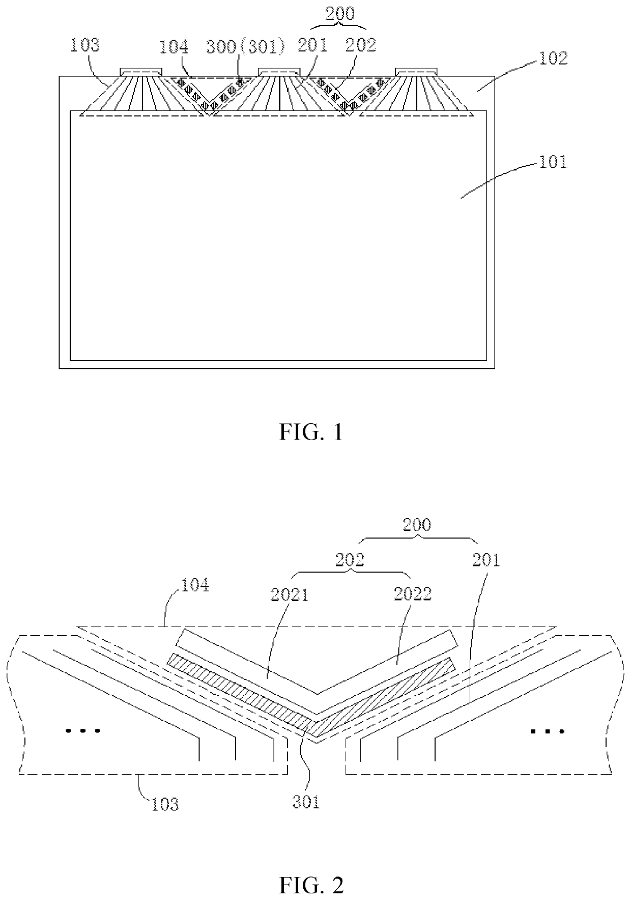
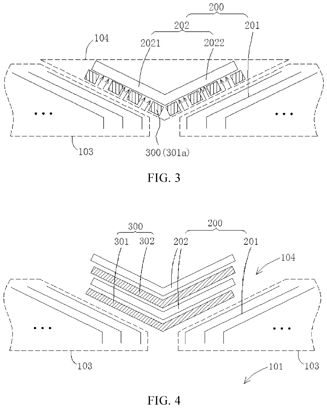
[0051]Referring to FIG. 1, it is a schematic structural view illustrating the array substrate of the present application. The array substrate comprises a display region 101 and a non-display region 102, wherein the non-display region 102 comprises a fan-out region 103 arranged on at least one side of the display region 101. In the present embodiment, a description is made by taking as an example that a plurality of fan-out regions 103 are provided at one side of the display region 101. An inverted triangle region 104 is formed between two adjacent fan-out regions 103 at the same side of the display region 101. The array substrate comprises a plurality of metal lines 200 and a plurality of floating metal lines 300, the metal lines 200 comprise a plurality of first metal lines 201 and a plurality of second metal lines 202, the first metal lines 201 are distributed in a fan shape in the fan-out region 103, and the second metal lines 202 are arranged in the inverted triangle region 104....

second embodiment

[0068]As shown in FIG. 4 and FIG. 5, the structure of the array substrate in the present embodiment is the same as or similar to that in the first embodiment above. The difference is that: at least two of the second metal lines 202 are sequentially arranged at intervals in a direction, from near to far, with respect to the display region 101. The floating metal lines 300 also comprise a plurality of second floating metal lines 302 arranged in the inverted triangle region 104, and the second floating metal line 302 is located between two adjacent second metal lines 202.

[0069]In the present embodiment, the orthographic projection of the metal lines 200 projected on the array substrate and the orthographic projection of the floating metal lines 300 projected on the array substrate do not overlap.

[0070]In the present embodiment, the second floating metal line 302 and the first floating metal line 301 have the same structural design. As shown in FIG. 4, it is a partial structural view il...

third embodiment

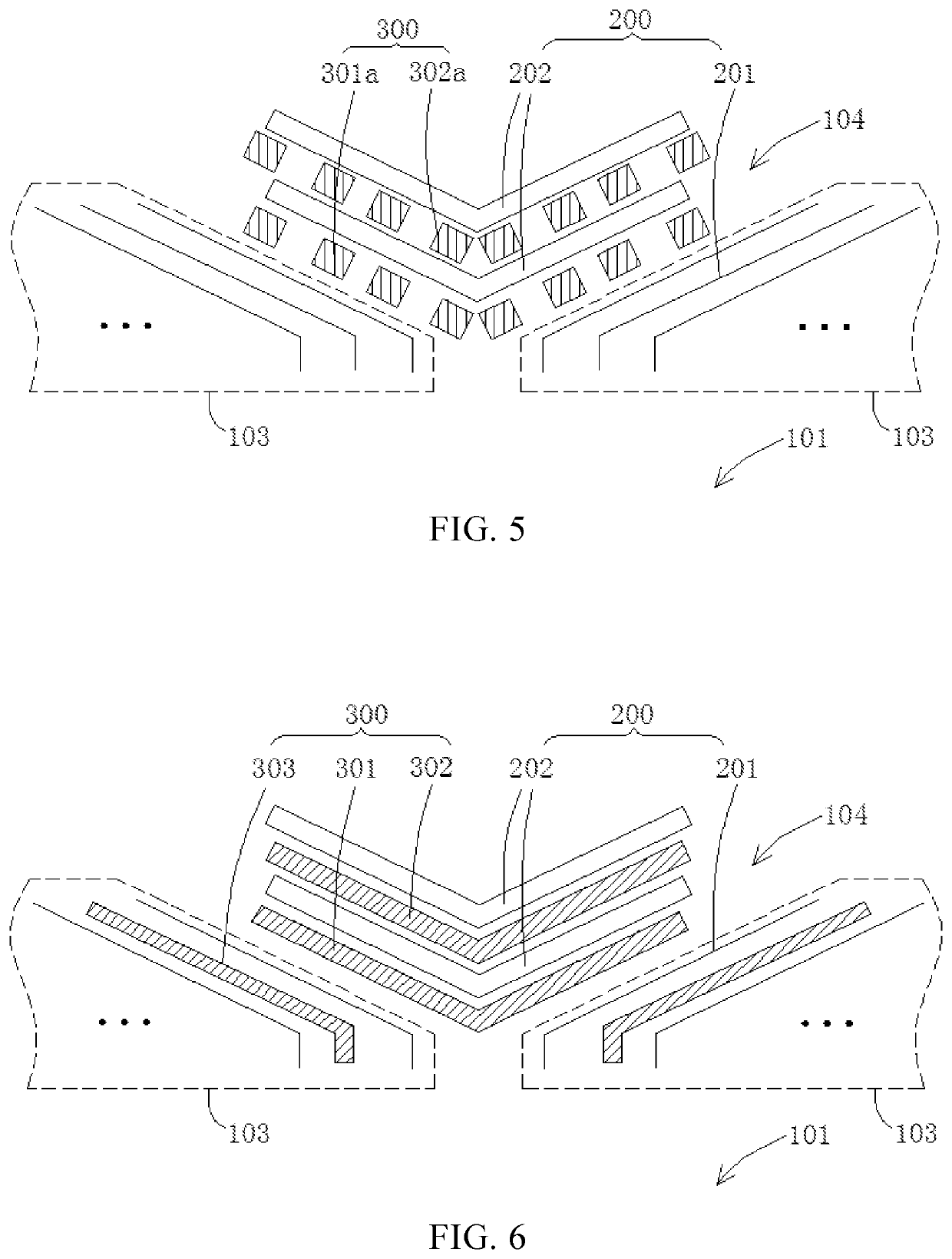
[0074]As shown in FIG. 6 and FIG. 7, the structure of the array substrate in the present embodiment is the same as or similar to that in the foregoing second embodiment. The difference is that the floating metal line 300 further comprises a third floating metal line 303 arranged in the fan-out region 103. The third floating metal line 303 is located between two adjacent first metal wires 201.

[0075]In the present embodiment, the orthographic projection of the metal lines 200 projected on the array substrate and the orthographic projection of the floating metal lines 300 projected on the array substrate do not overlap.

[0076]In the present embodiment, the third floating metal line 303 can have the same structural design as the second floating metal line 302 and the first floating metal line 301.

[0077]Specifically, as shown in FIG. 6, it is a partial structural view illustrating a first type of array substrate according to the third embodiment of the present application. The third float...


PUM

PropertyMeasurementUnit
distanceaaaaaaaaaa
distanceaaaaaaaaaa
distanceaaaaaaaaaa

Abstract

The present application provides an array substrate and a display panel. The array substrate includes fan-out regions and an inverted region formed between two adjacent fan-out regions. The array substrate includes metal lines and floating metal lines. The metal lines include first metal lines in the fan-out region and second metal lines in the inverted triangle region. The floating metal lines include a first floating metal line arranged between the first metal lines and the second metal lines. The array substrate includes an alignment film arranged on the metal lines and the floating metal lines.

Description

FIELD OF DISCLOSURE[0001]The present application relates to a field of display technology and in particular, to an array substrate and a display panel.DESCRIPTION OF RELATED ART[0002]With the development of flat panel display technology, there has been a trend to develop flat panel displays with high resolution, high contrast ratios, high refresh rate, narrow bezel, and thinness. At present, liquid crystal displays are still the mainstream products of flat panel displays. Especially now that all large-size flat panel displays have been developed to approach 8K resolution. To maintain the narrow bezels at extremely high resolutions while providing good display quality, there are a lot of challenges in manufacturing processes, such as coating an alignment film (PI) on one side of an array substrate.[0003]Generally, signal lines in a display region of an array substrate are connected to terminal pads at an edge of the array substrate through metal lines of the fan-out region, and an in...

Claims


Application Information

Patent Timeline
Patent Type & Authority Applications(United States)
IPC IPC(8): H01L27/12G02F1/1362
CPCH01L27/124H01L25/18G02F1/136286G02F1/1337G02F1/133357G02F2201/48G02F1/1345
Inventor XU, ZHIDA
Owner SHENZHEN CHINA STAR OPTOELECTRONICS SEMICON DISPLAY TECH CO LTD
Why Eureka
Try Eureka