
Semiconductor memory device and method of forming the same

Active Publication Date: 2022-06-30
FUJIAN JINHUA INTEGRATED CIRCUIT CO LTD
View PDF2 Cites 0 Cited by
  • Summary
  • Abstract
  • Description
  • Claims
  • Application Information

AI Technical Summary

Benefits of technology

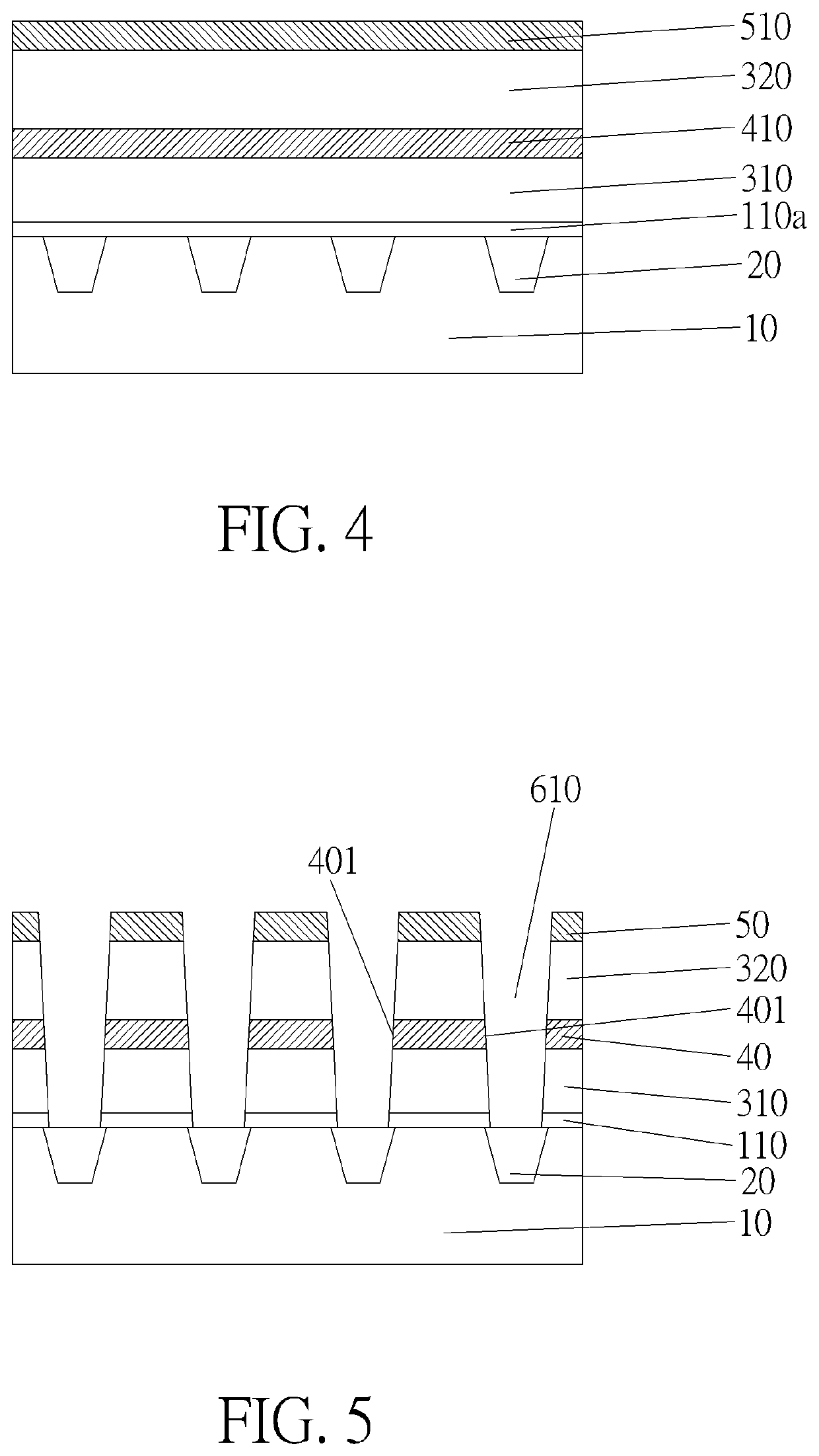
The present invention provides a fabricating method of a semiconductor memory device with improved performance. The method involves forming a stack structure on a substrate with a first sacrificial layer, a first supporting layer, and a second sacrificial layer, and then removing the sacrificial layers to form a second high-k dielectric layer which directly contacts the supporting layer in two directions perpendicular to the substrate. The resulting structure has improved performance and stability.

Problems solved by technology

However, with the continuous reduction of the device size, the size of the opening formed by breaking the supporting layers also gradually decreases, which greatly increases the aspect ratio of the opening.
While further filling in the required dielectric layer and the upper electrode in the opening in the subsequent processes, the fabricating difficulties are increased and the capacitance of the capacitor in the semiconductor memory is difficult to further increase accordingly.

Method used


Image

  • Semiconductor memory device and method of forming the same
  • Semiconductor memory device and method of forming the same
  • Semiconductor memory device and method of forming the same

Examples


Embodiment Construction

[0023]It should be noted that different embodiments or the technical features in different embodiments described in the following may be replaced, recombined, or mixed with one another without departing from the spirit of the present invention. The presented invention is described in detail with reference to the embodiments in the accompanying drawings.

[0024]For better understanding of the presented invention, the technical scheme in the embodiments of the present invention will be described clearly and completely with reference to the drawings in the embodiments of the present invention. Obviously, the described embodiments are only a part of the embodiments of the present invention, not all of them. According to the embodiments of the present invention, all other embodiments obtained by ordinary technicians in the arts without creative labor should belong to the protecting scope of the present invention.

[0025]It is understood that, although the terms first, second, etc. may be use...


PUM


Abstract

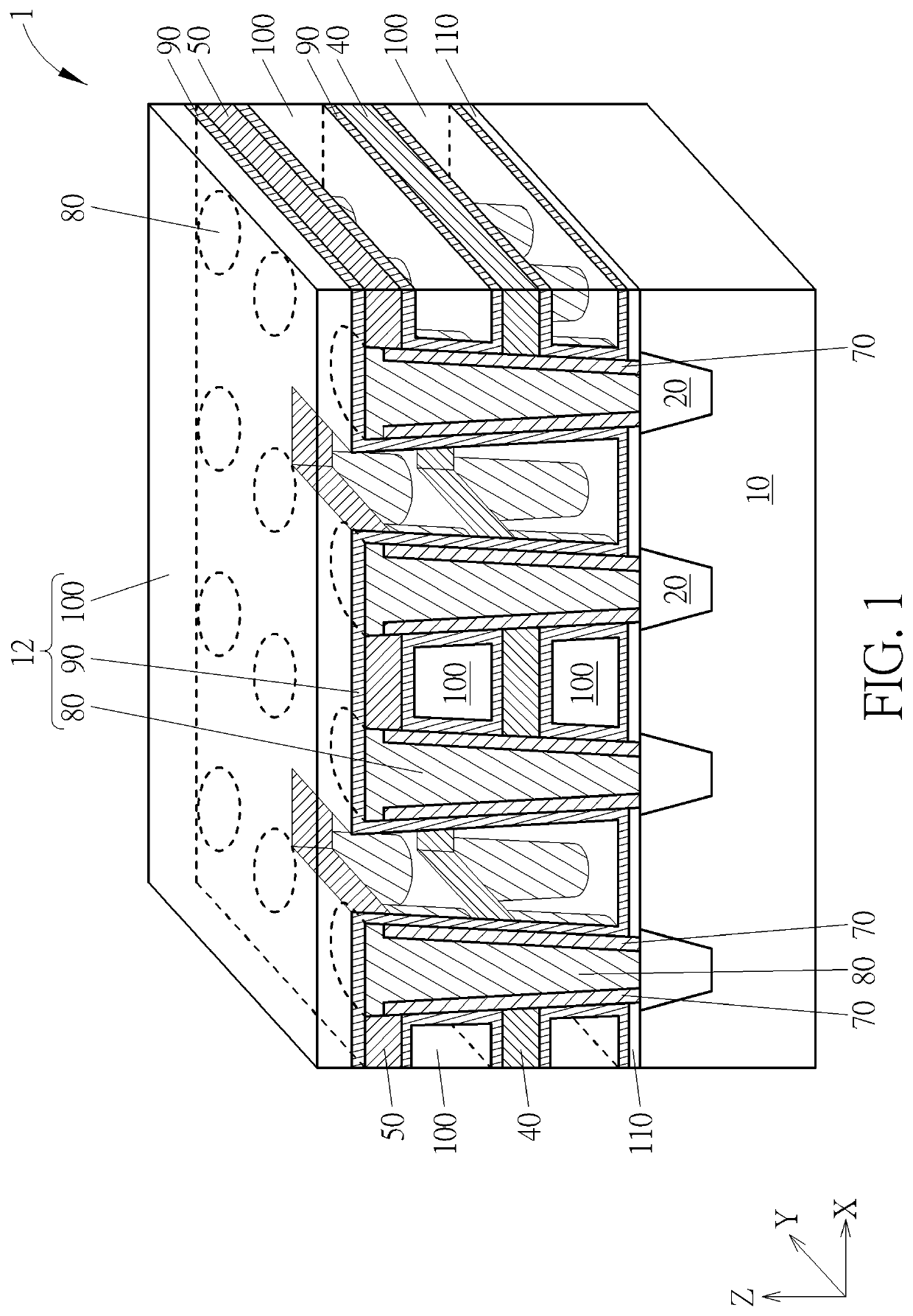
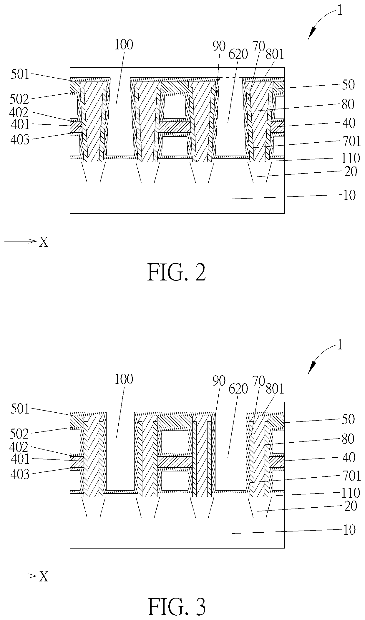
The present invention provides a semiconductor memory device and a fabricating method thereof. The semiconductor memory device includes a substrate, a plurality of capacitors and a supporting layer disposed on the substrate, wherein each of the capacitors is connected with at least one of the adjacent capacitors through the supporting layer. Each of the capacitors includes first electrodes, a high-k dielectric layer and a second electrode, and the high-k dielectric layer is disposed between the first electrodes and the second electrode. Due to the supporting layer directly contacts the high-k dielectric layer through a surface thereof, and the high-k dielectric layer completely covers the surface, the second electrode may be formed directly within openings with an enlarged dimension. Accordingly, the process difficulty of performing the deposition and etching processes within the openings may be reduced, and the capacitance of the capacitors is further increased.

Description

BACKGROUND OF THE INVENTION1. Field of the Invention[0001]The present invention generally relates to a semiconductor device and a forming method thereof, and more particularly to a semiconductor memory device and a forming method thereof.2. Description of the Prior Art[0002]A semiconductor memory device with capacitors is one of the necessary components in the integrated circuit, which provides functions of voltage adjustment, filtering, and the like.[0003]Capacitors are usually divided into horizontal capacitors and vertical capacitors. The vertical capacitors having a plurality of deep grooves filled with lower electrode materials in the substrate, so as to reduce the occupied area of the capacitors by providing the plate area of the capacitors through the sidewalls of the deep grooves, and also to obtain a larger capacitance at the same time.[0004]Recently, the current manufacturing process of the vertical capacitors generally includes: filling deep grooves with lower electrode m...

Claims


Application Information

Patent Timeline
IPC IPC(8): H01L49/02
CPCH01L28/91H01L28/90H10B12/033H01L28/60H10B20/50H10B41/20H10B41/30H10B43/20H10B43/30H10B51/20
Inventor TSAI, PEI-TINGTUNG, YU-CHENGLU, TSUO-WENCHEN, MIN-TENGCHEN, TSUNG-WEN
Owner FUJIAN JINHUA INTEGRATED CIRCUIT CO LTD
Learn More