
Method for fabricating first electrode of capacitor

Inactive Publication Date: 2008-03-06
PROMOS TECH INC
View PDF7 Cites 0 Cited by
  • Summary
  • Abstract
  • Description
  • Claims
  • Application Information

AI Technical Summary

Benefits of technology

[0014]Accordingly, at least one objective of the present invention is to provide a method for fabricating a first electrode of a capacitor capable of increasing the capacitance of the capacitor.
[0015]At least another objective of the present invention is to provide a method for fabricating a first electrode of a capacitor capable of increasing the production throughput and lowering the production cost.
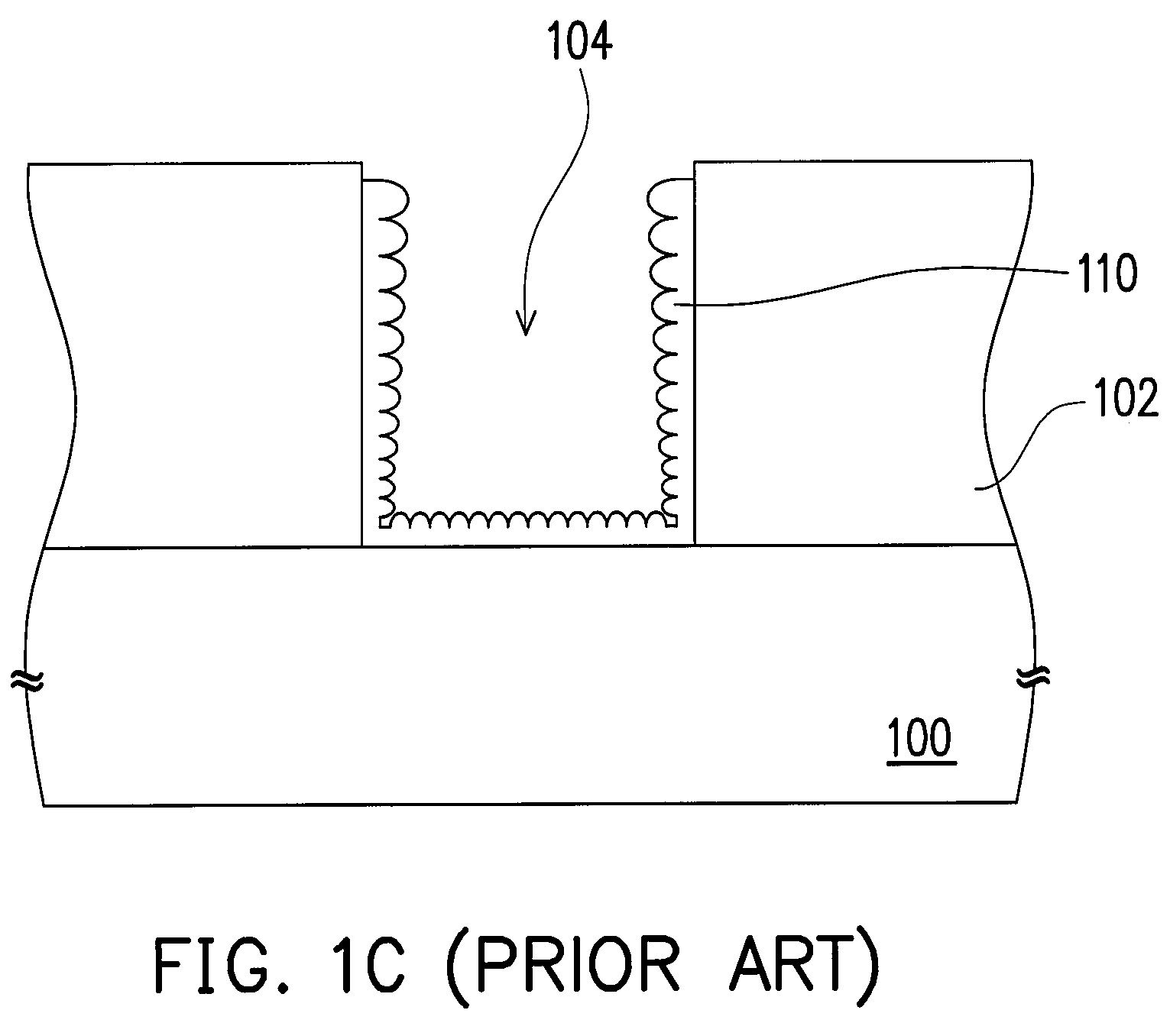
[0024]Accordingly, because a photoresist layer is not required for fabricating the first electrode of the capacitor in the present invention, and therefore the problem of incomplete removal of the photoresist layer or damaging the surface structure of the silicon layer during its exposure to plasma used for removal of the photoresist layer may be effectively avoided. Therefore, it is possible to form dimensionally uniform hemispherical grains inside the opening to effectively increasing the capacitance of the capacitor.
[0025]In addition, because a photoresist layer is not required for fabricating the first electrode of the capacitor in the present invention, and therefore there is no need to perform a series of processes including photoresist coating, exposure, development, photoresist removal and silicon layer cleaning. Therefore, the fabricating process is significantly simplified so that the production throughput can be increased and the production cost can be reduced.

Problems solved by technology

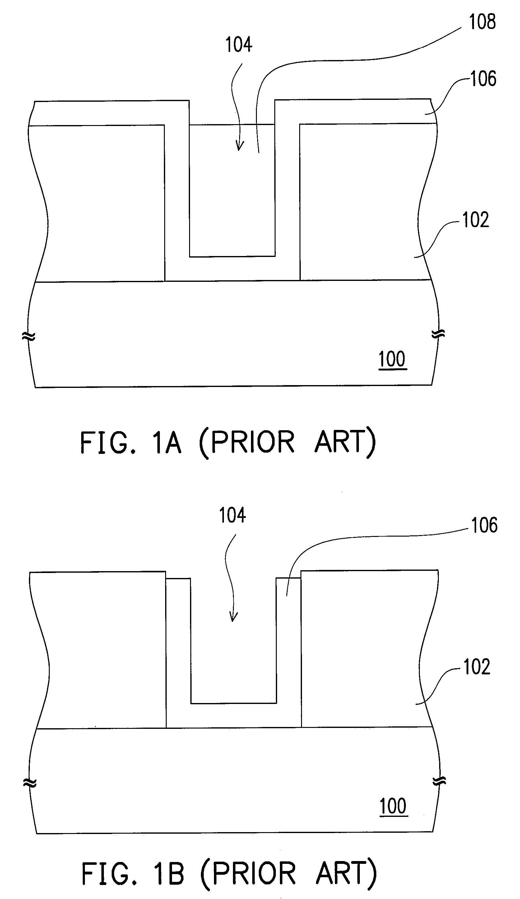
In addition, the conventional method of fabricating the first electrode of the capacitor is rather complicated.
Therefore, the inherent problems of having a longer production cycle and a higher production cost for producing the product are hard to remove.

Method used


Image

  • Method for fabricating first electrode of capacitor
  • Method for fabricating first electrode of capacitor
  • Method for fabricating first electrode of capacitor

Examples


Embodiment Construction

[0031]Reference will now be made in detail to the present preferred embodiments of the invention, examples of which are illustrated in the accompanying drawings. Wherever possible, the same reference numbers are used in the drawings and the description to refer to the same or like parts.

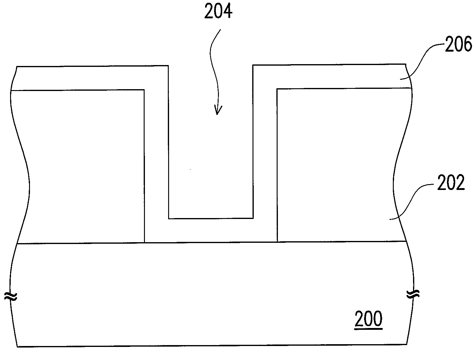
[0032]FIGS. 2A through 2C are schematic cross-sectional views showing the steps for fabricating a first electrode of a capacitor according to one embodiment of the present invention.

[0033]First, as shown in FIG. 2A, a substrate 200 comprising an insulating layer 202 formed thereon is provided. The insulating layer 202 has an opening 204. The substrate 200 may be comprised of a semiconductor substrate, for example. The insulating layer 202 is a silicon oxide and may be formed, for example, by performing a chemical vapor deposition process. The aspect ratio of the opening 204 is, for example, between 25 and 35. The method of forming the opening 204 includes, for example, performing a patterning process...


PUM


Abstract

A method for fabricating a first electrode of a capacitor is described. A substrate comprising an insulating layer formed thereon is provided. The insulating layer has an opening. A silicon layer is formed on the insulating layer. The silicon layer is transformed to a hemispherical grain layer. An etching process is performed to remove a portion of the hemispherical grain layer outside the opening.

Description

CROSS-REFERENCE TO RELATED APPLICATION[0001]This application claims the priority benefit of Taiwan application serial no. 95132699, filed Sep. 5, 2006. All disclosure of the Taiwan application is incorporated herein by reference.BACKGROUND OF THE INVENTION[0002]1. Field of the Invention[0003]The present invention relates to a method for fabricating a capacitor, and more particularly, to a method for fabricating a first electrode of a capacitor.[0004]2. Description of Related Art[0005]Semiconductor integrated circuits normally require capacitors, in particular, memory devices need capacitors so that each memory device is able to store binary data according to the degree of bias in the capacitor. For a memory device such as a dynamic random access memory (DRAM), the reading / writing actions of the DRAM are achieved through a transfer field effect transistor (TFET). The source of the transfer field effect transistor is electrically coupled to the bit line, the drain is electrically coup...

Claims


Application Information

Patent Timeline
IPC IPC(8): H01L21/8244
CPCH01L27/10808H01L28/84H01L27/10852H10B12/31H10B12/033
Inventor TENG, LI-CHENGYU, CHUN-WEIFU, CHUN-CHONGCHANG, YUAN-MING
Owner PROMOS TECH INC
Learn More