
Semiconductor device and method for fabricating the same using damascene process

a damascene and semiconductor technology, applied in semiconductor devices, capacitors, electrical devices, etc., can solve the problems of increasing the difficulty of ensuring the process margin of a semiconductor device, increasing the difficulty of process, and many problems, so as to improve the process margin, simplify the fabrication process, and increase the capacitance of a capacitor

Inactive Publication Date: 2007-05-15
SAMSUNG ELECTRONICS CO LTD
View PDF9 Cites 2 Cited by
  • Summary
  • Abstract
  • Description
  • Claims
  • Application Information

AI Technical Summary

Benefits of technology

[0019]Embodiments of the invention provide a semiconductor device and a method for fabricating the semiconductor device by forming the storage node contact and then forming the bit line pattern, thereby improving the process margin while maintaining the dielectric property between a storage node contact and a bit line.
[0020]Another embodiment of the invention provides a semiconductor device and a method for fabricating the semiconductor device by simultaneously forming a damascene bit line and a storage node contact plug, thereby simplifying the fabrication process.
[0021]Yet another embodiment of the invention provides a semiconductor device and a method for fabricating the semiconductor device that is capable of increasing the capacitance of a capacitor along as well as increasing the storage node area.

Problems solved by technology

Accordingly, etching the interconnection causes many problems.
It has become more difficult to assure a process margin for a semiconductor device having a capacitor on a bit line COB structure while simultaneously maintaining the required dielectric properties between a storage node contact and bit line.
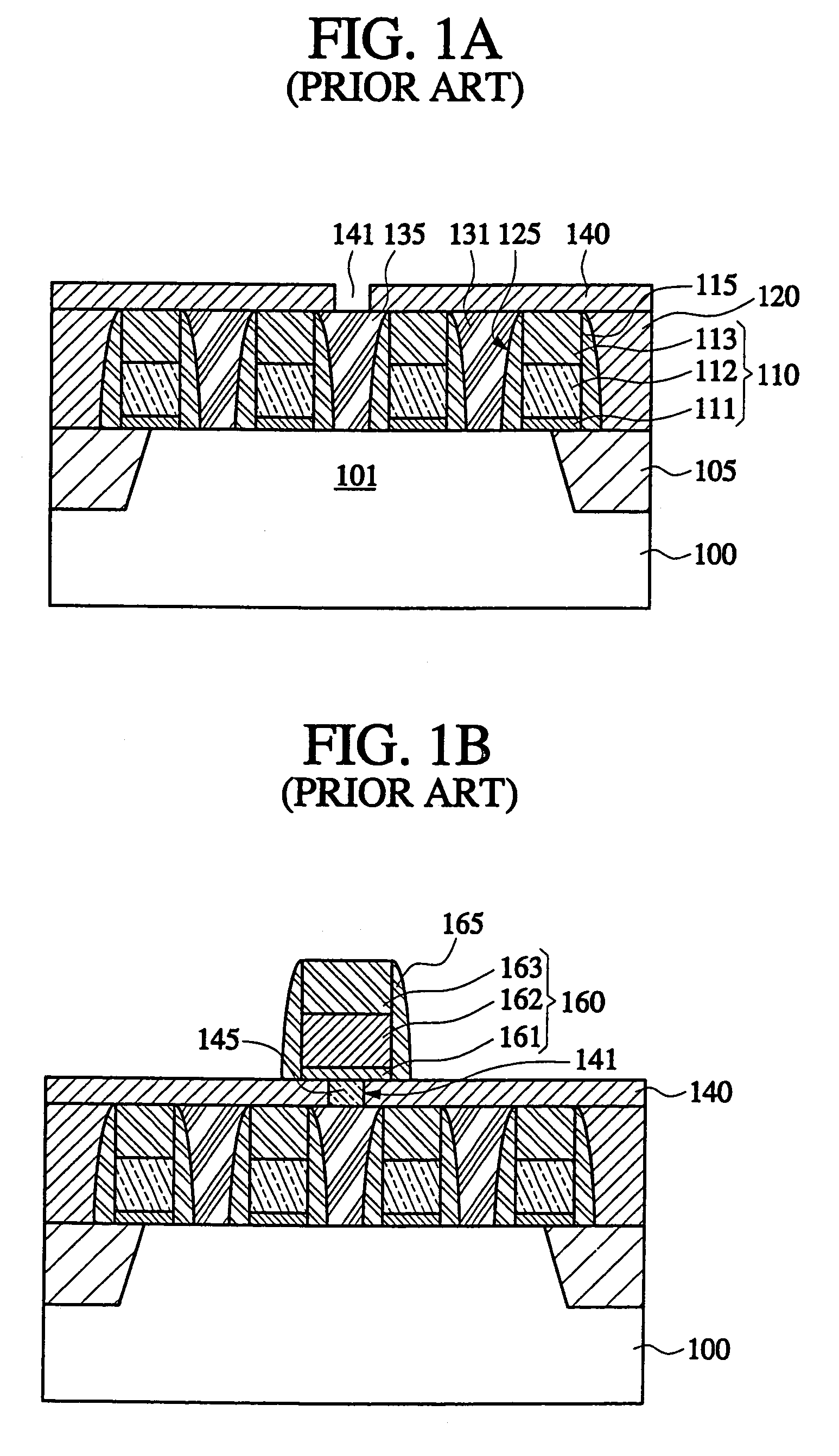
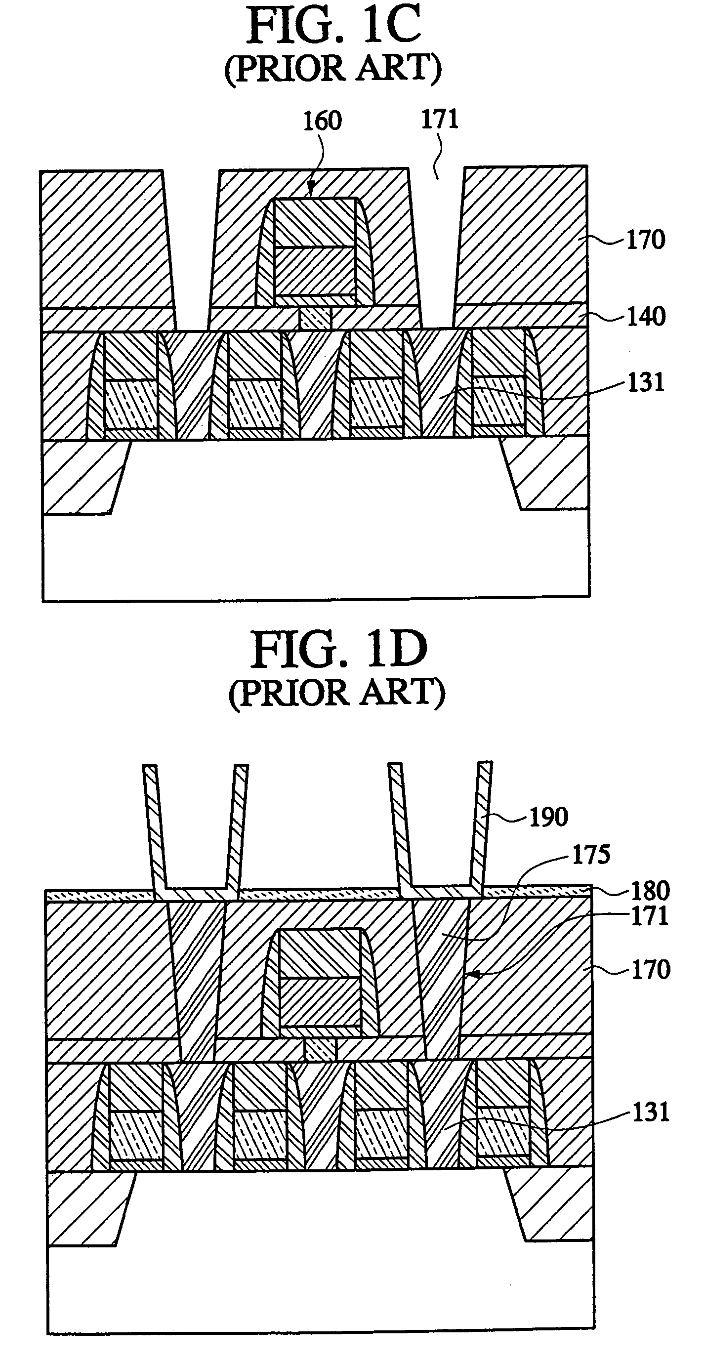
As described above, since the conventional method for fabricating the semiconductor device to form bitlines includes depositing and patterning of metal film, the process is very complicated and very difficult.
Also, it is difficult to assure the process margin while maintaining the required dielectric properties between a storage node contact and the bit line during the formation of the storage node contact.

Method used


Image

  • Semiconductor device and method for fabricating the same using damascene process
  • Semiconductor device and method for fabricating the same using damascene process
  • Semiconductor device and method for fabricating the same using damascene process

Examples


Embodiment Construction

[0026]The semiconductor device and method for fabricating the device according to the embodiments of the invention will now be described with reference to the accompanying drawings.

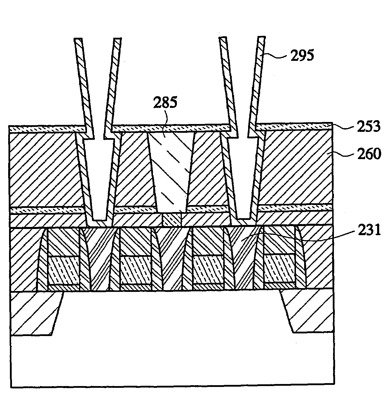
[0027]FIGS. 2A through 2I are cross sectional diagrams illustrating a method of fabricating a semiconductor device having a COB structure according to an embodiment of the invention.

[0028]Referring to FIG. 2A, a semiconductor substrate 200 includes an active region 201 and a field region (not shown). A field isolation film 205 is formed in the field region of the semiconductor substrate 200 through a conventional shallow trench isolation STI process.

[0029]A gate 210 having a stack structure of a gate insulating film 211, a gate electrode material 212, and a capping layer 213 is formed on the semiconductor substrate 100. A spacer 215 is formed on the sidewall of the gate 210.

[0030]A first interlayer insulating film 220 is deposited on the substrate including the gate 210 and is planarized by a CMP process ...


PUM


Abstract

A semiconductor device and method for fabricating same according to an embodiment of the invention includes: preparing a semiconductor substrate having a first contact pad and a second contact pad; forming a first insulating film on the substrate; etching the first insulating film to form a groove-shaped bit line pattern and a contact exposing the first contact pad and the second contact pad, respectively; simultaneously forming a contact plug and a bit line in the contact and the bit line pattern, respectively, the contact plug and the bitline having upper surfaces that are coplanar; and forming a bottom electrode for a capacitor that is connected to the first contact pad.

Description

CROSS REFERENCE TO RELATED APPLICATIONS[0001]This application claims priority from Korean Patent Application No. 2002-63979, filed on Oct. 18, 2002 in the Korean Intellectual Property Office, the contents of which are hereby incorporated by reference in their entirety.BACKGROUND OF THE INVENTION[0002]1. Field of the Invention[0003]This disclosure relates to a semiconductor device, and more particularly to a semiconductor device and method for fabricating the semiconductor device with damascene bit lines that improves the process margin and simplifies the fabrication process.[0004]2. Description of the Related Art[0005]As the size of semiconductor devices decrease, interconnections of the semiconductor devices become finer. Accordingly, etching the interconnection causes many problems. It has become more difficult to assure a process margin for a semiconductor device having a capacitor on a bit line COB structure while simultaneously maintaining the required dielectric properties bet...

Claims


Application Information

Patent Timeline
Patent Type & Authority Patents(United States)
IPC IPC(8): H01L21/8242H10B12/00H01L21/02H01L21/28H01L21/311H01L21/4763H01L21/60H01L21/768
CPCH01L27/10852H01L28/91H01L21/31116H01L27/10814H01L27/10855H01L27/10885H10B12/315H10B12/033H10B12/0335H10B12/482H10B99/00
Inventor LEE, CHANG-HUHNJEONG, MUN-MO
Owner SAMSUNG ELECTRONICS CO LTD
Learn More