Check patentability & draft patents in minutes with Patsnap Eureka AI!

Substrate fixing device

Pending Publication Date: 2022-07-14
SHINKO ELECTRIC IND CO LTD
View PDF0 Cites 0 Cited by
  • Summary
  • Abstract
  • Description
  • Claims
  • Application Information

AI Technical Summary

Benefits of technology

The invention is a device that fixes a substrate, which helps to make the temperature of the substrate even across its surface. This improves the performance of the substrate during processing.

Problems solved by technology

The substrate fixing device according to the background art may not be able to obtain sufficient heat uniformity in an adsorption face of the electrostatic adsorption member.

Method used


Image

  • Substrate fixing device
  • Substrate fixing device
  • Substrate fixing device

Examples


first embodiment

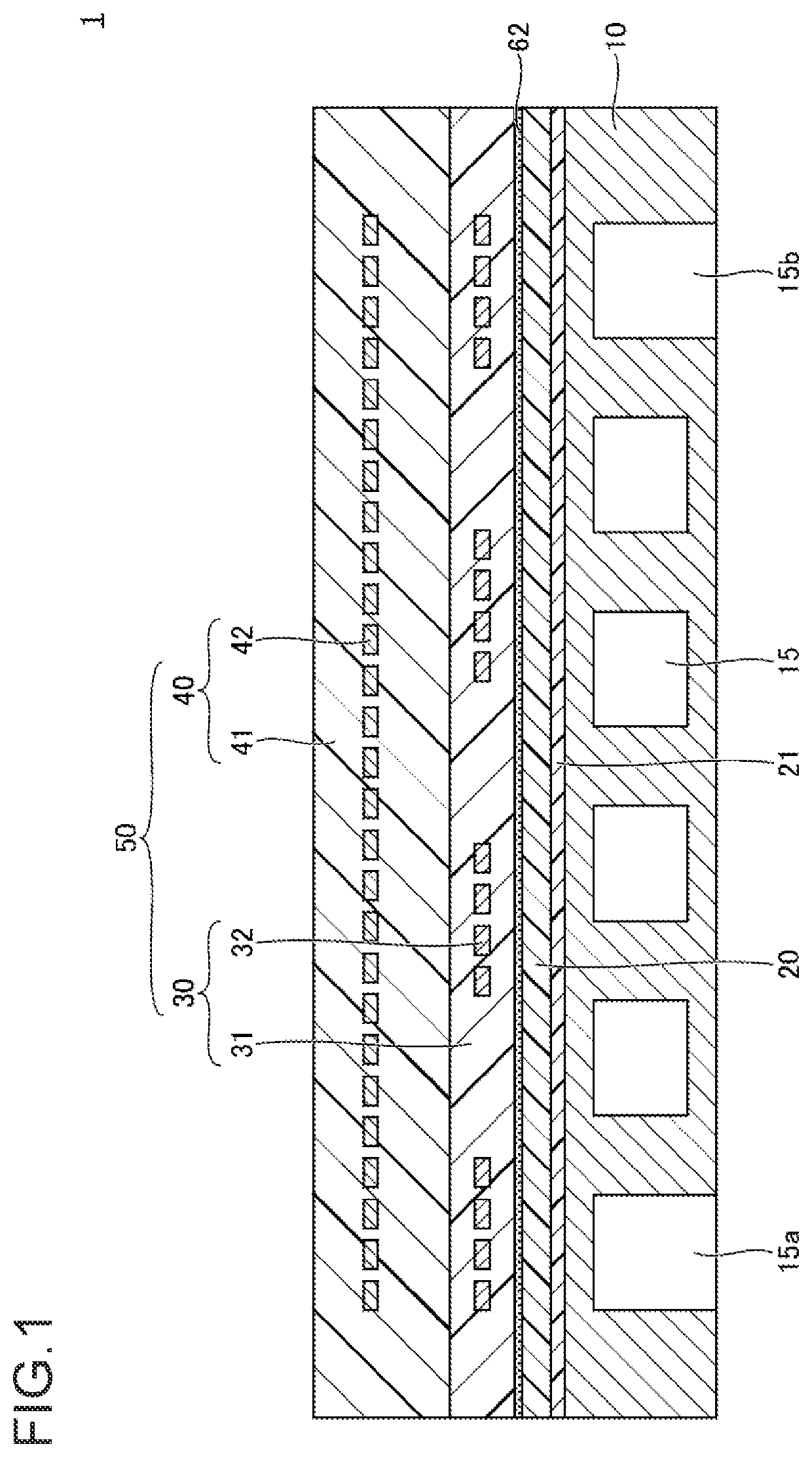
[0017]First, a first embodiment will be described. FIG. 1 is a sectional view showing a substrate fixing device according to the first embodiment.

[0018]As shown in FIG. 1, the substrate fixing device 1 according to the first embodiment has a base plate 10, an adhesive layer 20, an auxiliary adhesive layer 21, and an electrostatic adsorption member 50 as major constituent elements.

[0019]The base plate 10 is a member for mounting the electrostatic adsorption member 50 thereon. Thickness of the base plate 10 can be, for example, set in a range of about 20 mm to 50 mm. The base plate 10 is, for example, formed from aluminum, and can be also used as an electrode or the like for controlling plasma. By feeding predetermined high-frequency electric power to the base plate 10, energy for making ions or the like in a generated plasma state collide against a substrate such as a wafer adsorbed on the electrostatic adsorption member 50 can be controlled to effectively perform an etching process....

second embodiment

[0048]Next, a second embodiment will be described. The second embodiment mainly differs from the first embodiment in a configuration of an electrostatic adsorption member. FIG. 6 is a sectional view showing a substrate fixing device according to the second embodiment.

[0049]In the substrate fixing device 2 according to the second embodiment, as shown in FIG. 6, the electrostatic adsorption member 50 does not include a heating portion 30, but a heating element 32 is built in an electrostatic chuck 40. The remaining configuration is similar to or the same as that according to the first embodiment.

[0050]An effect similar to or the same as that according to the first embodiment can be obtained also by the second embodiment.

third embodiment

[0051]Next, a third embodiment will be described. The third embodiment mainly differs from the first embodiment in a configuration of a portion between a base plate 10 and an electrostatic adsorption member 50. FIG. 7 is a sectional view showing a substrate fixing device according to the third embodiment.

[0052]In the substrate fixing device 3 according to the third embodiment, as shown in FIG. 7, a primer layer 61 is applied to a face of the base plate 10 on the electrostatic adsorption member 50 side. The primer layer 61 may, for example, contain titanium. The substrate fixing device 3 does not include an auxiliary adhesive layer 21, but an adhesive layer 20 directly contacts the primer layer 61. The remaining configuration is similar to or the same as that according to the first embodiment. The primer layer 61 is an example of a first primer layer.

[0053]An effect similar to or the same as that according to the first embodiment can be obtained also by the third embodiment. In addit...


PUM


Abstract

A substrate fixing device includes: a base plate; an electrostatic adsorption member that adsorbs and holds a substrate; and a first adhesive layer that adhesively bonds the electrostatic adsorption member to the base plate. A storage modulus of the first adhesive layer is not less than 0.01 MPa and not more than 25 MPa within a temperature range of −110° C. to 250° C.

Description

[0001]This application claims priority from Japanese Patent Applications No. 2021-004453, filed on Jan. 14, 2021, and No. 2021-104338, filed on Jun. 23, 2021, the entire contents of which are herein incorporated by reference.BACKGROUNDTechnical Field[0002]The present disclosure relates to a substrate fixing device.Background Art[0003]In a substrate fixing device used for fixation of a substrate such as a wafer, an electrostatic adsorption member is typically adhesively bonded to a base plate by an adhesive layer (see e.g., WO2016 / 035878, JP-A-2014-207374, WO2009 / 107701, JP-A-2011-091297, JP-A-2020-023088. JP-A-2015-061913, JP-A-2019-220503, and JP-A-2007-299837).[0004]The substrate fixing device according to the background art may not be able to obtain sufficient heat uniformity in an adsorption face of the electrostatic adsorption member. In other words, temperature of the adsorption face of the electrostatic adsorption member may vary.SUMMARY[0005]One of aspects of the present dis...

Claims


Application Information

Patent Timeline
IPC IPC(8): H01L21/683
CPCH01L21/6833H01L21/68757H01L21/68785H01L21/67109B23Q3/15H02N13/00
Inventor SATO, KEITAYANAGISAWA, HIROHARUYAMADA, YOHEINAKAMURA, YUICHIIIJIMA, NOBUYUKI
Owner SHINKO ELECTRIC IND CO LTD
Features
  • R&D
  • Intellectual Property
  • Life Sciences
  • Materials
  • Tech Scout
  • Unparalleled Data Quality
  • Higher Quality Content
  • 60% Fewer Hallucinations
Learn More