

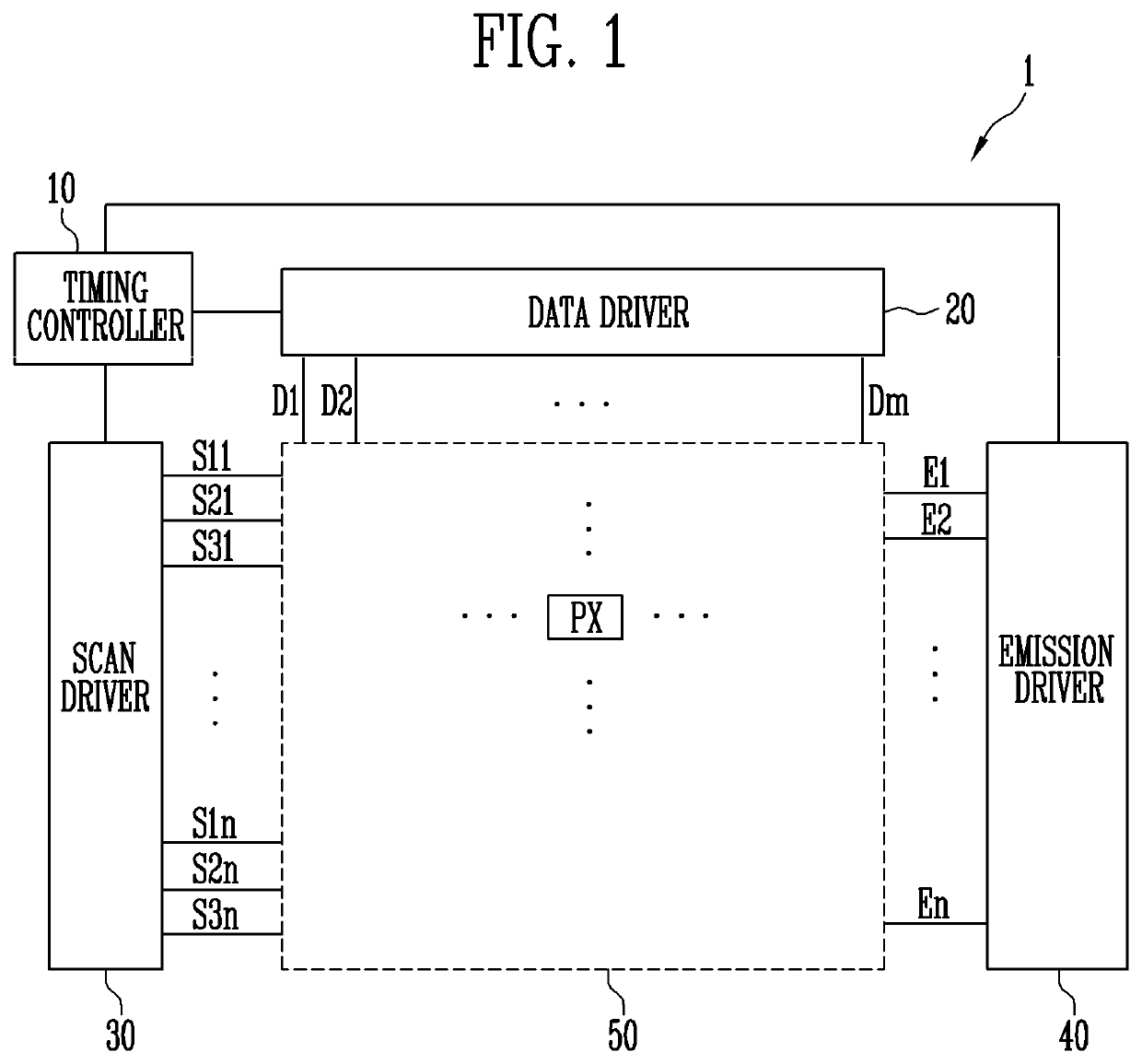
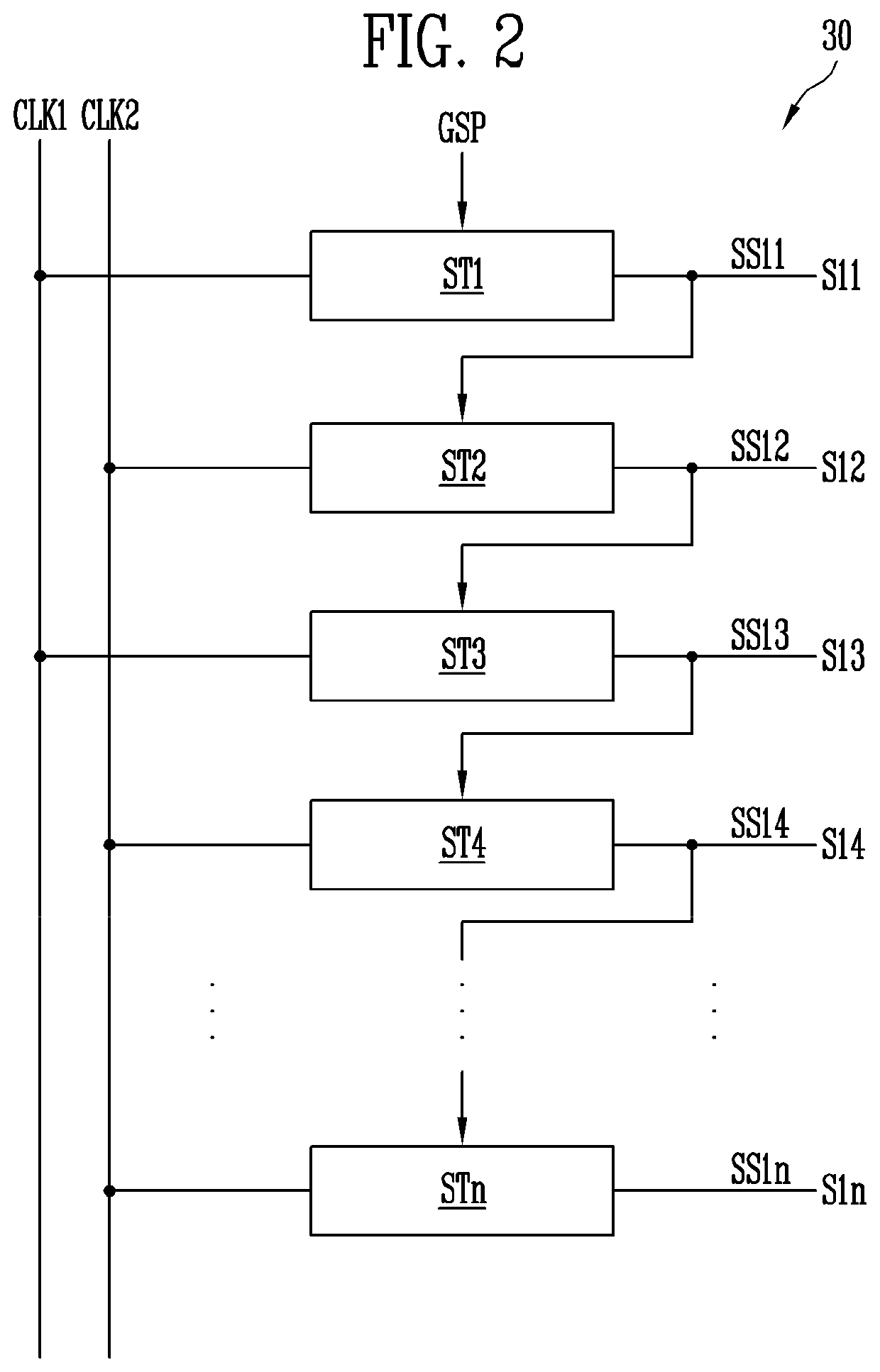
Pixels, display device comprising pixels, and driving method therefor
a technology of display device and driving method, which is applied in the direction of instruments, static indicating devices, etc., can solve the problem of certain leakage current generated in the driving transistor
- Summary
- Abstract
- Description
- Claims
- Application Information
AI Technical Summary
Benefits of technology
Problems solved by technology
Method used
Image

Examples
first embodiment
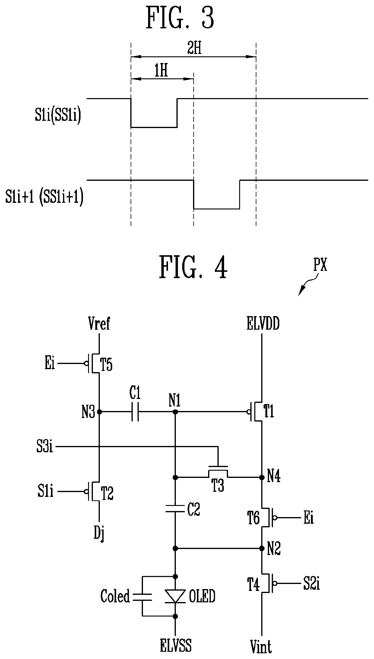
[0071]FIG. 4 is a circuit diagram of a pixel, according to the present disclosure. In FIG. 4, for convenience of explanation, the pixel PX located on an i-th horizontal line and connected to a j-th data line Dj will be taken as an example.
[0072]Referring to FIG. 4, the pixel PX includes first to sixth transistors T1 to T6, first and second capacitors C1 and C2, and an organic light emitting diode OLED.
[0073]The first transistor T1 is connected between a first driving power source ELVDD and a terminal of the sixth transistor T6, i.e., a fourth node N4. A gate electrode of the first transistor Ti is connected to a first node N1. The first transistor Ti may be turned on according to a voltage applied to the first node N1 to control an amount of a current flowing from the first driving power source ELVDD to the organic light emitting diode OLED through the sixth transistor T6. In various embodiments of the present disclosure, the first transistor T1 may be termed as a driving transistor...
second embodiment
[0138]In the present disclosure, the fourth transistor T4_1 is connected between the second node N2 and the initialization voltage Vint. A gate electrode of the fourth transistor T4_1 is connected to a second scan line S2i_1. The fourth transistor T4_1 may be turned on in response to a second scan signal applied to the second scan line S2i_1. When the fourth transistor T4_1 is turned on, the initialization voltage Vint may be applied to the second node N2, i.e., an anode electrode of the organic light emitting diode OLED.
[0139]In this embodiment of the present disclosure, a scan signal with a first polarity may be supplied for the first scan line S1i and scan signals with a second polarity may be supplied to the second and third scan lines S2i_1 and S3i.
[0140]In FIG. 14, in the high-frequency operation as shown in FIG. 5 and the low-frequency operation as shown in FIG. 6, operation in an arbitrary frame including the data write period WP and the emission period EP is shown. The arb...
third embodiment
[0146]In the present disclosure, the fourth transistor T4_2 is connected between the second node N2 and the initialization voltage Vint. The gate electrode of the fourth transistor T4_2 is connected to the (i+1)-th third scan line S3i+1. The fourth transistor T4_2 may be turned on in response to a third scan signal applied to the (i+1)-th third scan line S3i+1. When the fourth transistor T4_2 is turned on, the initialization voltage Vint may be applied to the second node N2, i.e., an anode electrode of the organic light emitting diode OLED.
[0147]In this embodiment, a scan signal with a first polarity may be supplied for the first scan line S1i and a scan signal with a second polarity may be supplied to the third scan line S3i and S3i+1.
[0148]In FIG. 16, in the high-frequency operation as shown in FIG. 5 and the low-frequency operation as shown in FIG. 6, operation in an arbitrary frame including the data write period WP and the emission period EP is shown. The arbitrary frame may be...
PUM
 Abstract
Description
Claims
Application Information