Composite recording structure for an improved write profermance
a recording structure and write profermance technology, applied in the field of magnetoresistive elements, can solve the problems of long write latency, small energy efficiency, rapid decrease of pma, etc., and achieve the effect of large spin transfer torque, high damping constant, and high spin polarization degrees
- Summary
- Abstract
- Description
- Claims
- Application Information
AI Technical Summary
Benefits of technology
Problems solved by technology
Method used
Image
Examples
first embodiment
of Current Invention
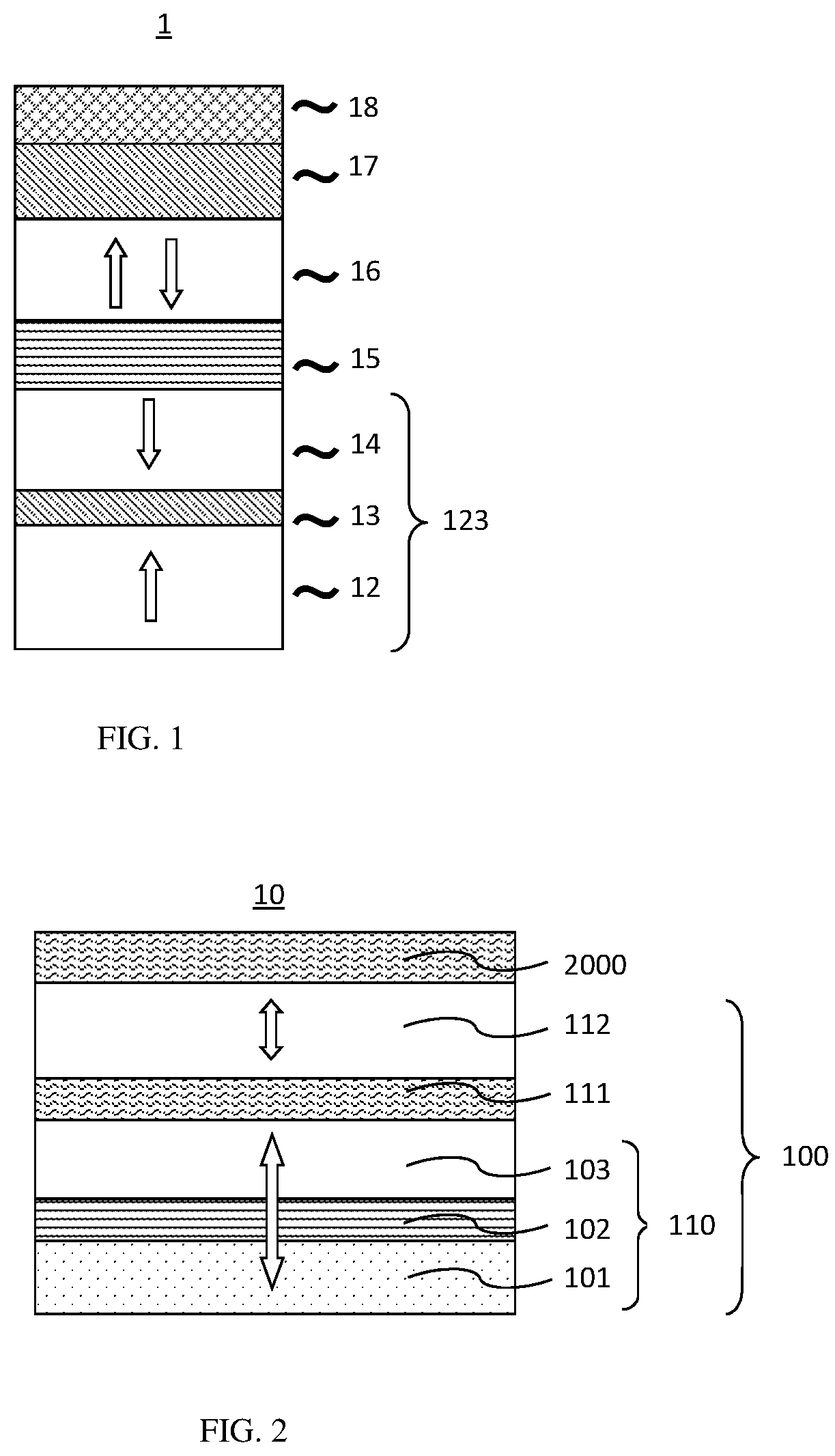
[0037]FIG. 2 is a cross-sectional view showing a configuration of a composite recording structure 1000 and a cap layer 2000 as deposited according to the first embodiment in this invention. The composite recording structure 1000 is configured by stacking a first free layer (FL1) 110, a nonmagnetic spacing layer 111 and a second free layer (FL2) 112, in the order from the bottom to the top. The first free layer consists of an amorphous magnetic material sub-layer 101, a Boron-absorbing material sub-layer 102 atop the amorphous magnetic material sub-layer and a Co / Ni superlattice sub-layer 103 atop the Boron-absorbing material sub-layer. Further, the cap layer 2000 is provided atop the composite recording structure 1000.
[0038]The amorphous magnetic material sub-layer 101 is made of CoFeB, CoFeB / Fe, CoB / Fe, CoFe / CoFeB, FeB / CoFe, CoB / CoFe or CoFeB / CoFe. The Boron-absorbing material sub-layer 102 is made of a metal or metal alloy containing at least one element select...
second embodiment
of Current Invention
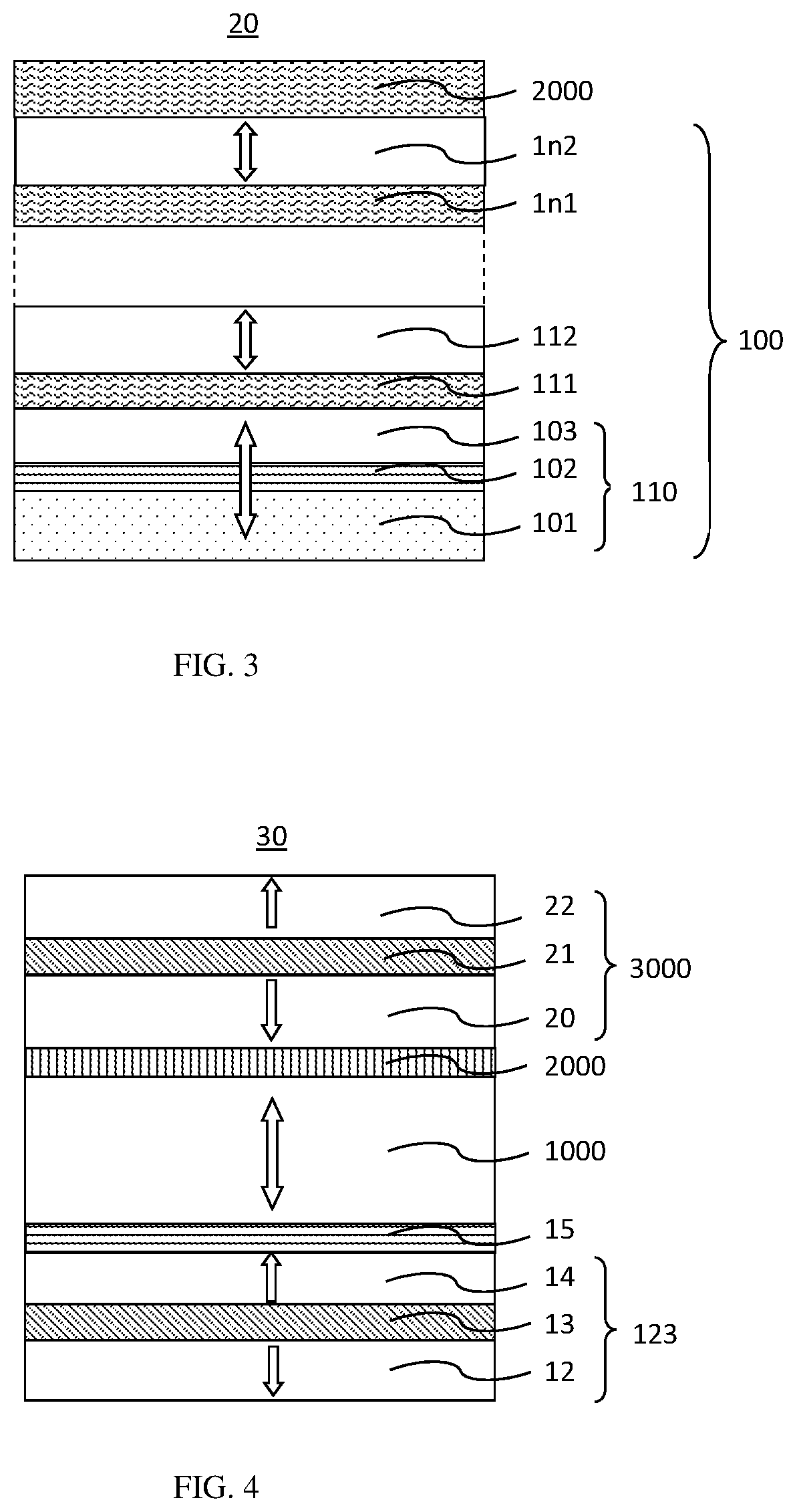
[0040]FIG. 3 is a cross-sectional view showing a configuration of a composite recording structure and a cap layer as deposited according to the second embodiment in this invention. The composite recording structure 1000 is configured by stacking a first free layer (FL1) 110, many repeats of a substructure including a nonmagnetic spacing layer and a Co / Ni superlattice free layer, in the order from the bottom to the top. The first free layer consists of an amorphous magnetic material sub-layer 101, a Boron-absorbing material sub-layer 102 atop the amorphous magnetic material sub-layer and a Co / Ni superlattice sub-layer 103 atop the Boron-absorbing material sub-layer. The first substructure consists a first nonmagnetic spacing layer 111 and a second free layer 112, the n-th substructure consists of a n-th nonmagnetic spacing layer 1n1 and a (n+1
[0041])-th free layer 1n2. Further, the cap layer 2000 is provided atop the composite recording structure 1000.
[0042]Simila...
third embodiment
of Current Invention
[0044]FIG. 4 is a cross-sectional view showing an example configuration of a magnetoresistive element 30 as deposited according to the third embodiment. The magnetoresistive element 30 is configured by stacking a reference structure 123, a tunnel barrier layer 15, a composite recording structure 1000, a cap layer 2000 and a magnetic STT-enhancing structure 3000 in the order from the bottom to the top. The reference structure 123 consists of a bottom pinning layer 12, an anti-ferromagnetic coupling (AFC) layer 13 and a reference layer 14. The composite recording structure 1000 consists of a first free layer and many repeats of a substructure including a nonmagnetic spacing layer and a Co / Ni superlattice free layer (not shown here). The magnetic STT-enhancing structure 3000 comprises a first magnetic material layer 20 having a magnetization direction parallel to the magnetization direction of the reference layer, a second AFC coupling layer 21 and a second magnetic...
PUM
 Abstract
Description
Claims
Application Information

