Unlock instant, AI-driven research and patent intelligence for your innovation.

Non-volatile memory circuit, semiconductor device, and method of reading non-volatile memory

a non-volatile memory and semiconductor technology, applied in the direction of static storage, digital storage, instruments, etc., can solve the problem of inability to set the expected threshold valu

Pending Publication Date: 2022-08-11
LAPIS TECH CO LTD
View PDF3 Cites 0 Cited by
  • Summary
  • Abstract
  • Description
  • Claims
  • Application Information

AI Technical Summary

Benefits of technology

The patent text describes a problem with a non-volatile memory circuit that uses a Zener zap element. The issue is that the threshold value that determines if the data is "0" or "1" based on the current flow through the Zener zap element cannot be set consistently due to dispersion in the resistance values. This results in cases where the expected threshold value cannot be achieved. The patent aims to address this problem and provide a more reliable and consistent method for setting the threshold value in such memory circuits.

Problems solved by technology

However, in a non-volatile memory circuit that uses an existing Zener zap element, the threshold value is set by a laser repair process, and there is dispersion in the values of the resistance that set the threshold value, and there are cases in which an expected threshold value cannot be set.

Method used


Image

  • Non-volatile memory circuit, semiconductor device, and method of reading non-volatile memory
  • Non-volatile memory circuit, semiconductor device, and method of reading non-volatile memory
  • Non-volatile memory circuit, semiconductor device, and method of reading non-volatile memory

Examples


first embodiment

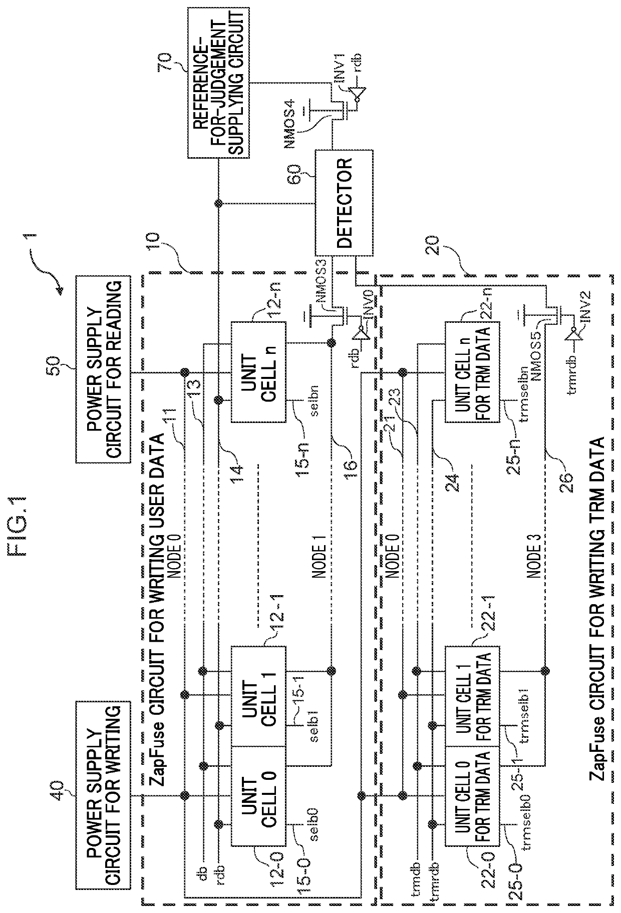
[0050]FIG. 1 is a drawing showing an example of the circuit structure of non-volatile memory circuit 1 relating to a first embodiment of the present disclosure.

[0051]The non-volatile memory circuit 1 that is shown in FIG. 1 has the power supply circuit 40 for writing, the power supply circuit 50 for reading, the power supply line 11 (also called node 0 hereinafter) for selectively supplying voltage for writing data from the power supplying circuit 40 for writing or voltage for reading data from the power supply circuit 50 for reading, the unit cells 12-1-12-n that are respectively connected in parallel between the power supply line 11 and an unillustrated reference power supply line that is connected to ground level, and that serve as n+1 (n is an integer of 1 or more) storage element portions that store data of 1 bit, the signal lines 13, 14, 15-0-15-n that input respective signals (db, rdb, selb0-selbn), which have been inputted from a control section provided at the exterior, to ...

second embodiment

[0082]FIG. 7 is a drawing showing an example of the circuit structure of a non-volatile memory circuit 2 relating to a second embodiment of the present disclosure.

[0083]The non-volatile memory circuit 2 shown in FIG. 7 is a structure in which a third storage section 30 is added to the non-volatile memory circuit 1 shown in FIG. 1.

[0084]The third storage section 30 in the non-volatile memory circuit 2 shown in FIG. 7 has a power supply line 31, unit cells 32-0-32-n that are respectively connected in parallel between the power supply line 31 and an unillustrated reference power supply line that is connected to ground level, and that serve as n+1 (n is an integer of 1 or more) storage element portions that store data of 1 bit, signal lines 33, 34, 35-0-35-n that input respective signals (trmdb, trmrrdb, trmselb0-trmselbn), which have been inputted from a control section provided at the exterior, to the respective unit cells 32-0-32-n, an output line (hereinafter also called node 4) 36 ...


PUM


Abstract

A non-volatile memory circuit includes: a first memory including a plurality of cells that store values by respectively having elements whose states change physically due to application of a voltage from an exterior, a second memory including a plurality of cells that store values by respectively having the elements, a detector that, at a time of reading from the first memory, judges a value stored in each of the cells by comparing a threshold value and current values from the plurality of cells and a judging circuit supplying current of a predetermined current value to the detector as the threshold value.

Description

CROSS-REFERENCE TO RELATED APPLICATION[0001]This application is based on and claims priority under 35 USC 119 from Japanese Patent Application No. 2021-018403 filed on Feb. 8, 2021, the disclosure of which is incorporated by reference herein.BACKGROUNDTechnical Field[0002]The present disclosure relates to a non-volatile memory circuit, a semiconductor device, and a method of reading a non-volatile memory.Related Art[0003]As disclosed in Japanese Patent Application Laid-Open (JP-A) No. 2003-204069 for example, in a Zener zap element, a zap diode is structured such that a P well region is formed at the surface layer of an N semiconductor layer, and a P anode region and an N cathode region are formed within the P well region, and an anode electrode and a cathode electrode are connected to the P anode region and the N cathode region respectively. Due to reverse bias voltage that is greater than or equal to the breakdown voltage being applied to the zap diode, the PN junction breaks-down...

Claims


Application Information

Patent Timeline
Patent Type & Authority Applications(United States)
IPC IPC(8): G11C11/4096G11C11/4074G11C11/4072G11C11/4076G11C29/44
CPCG11C11/4096G11C11/4074G11C29/4401G11C11/4076G11C11/4072G11C16/34G11C5/147G11C16/26G11C17/06G11C17/18G11C29/028G11C29/50008G11C29/006
Inventor MATSUMOTO, TAKUYA
Owner LAPIS TECH CO LTD