Packaged half-bridge circuit

a half-bridge circuit and bridge connection technology, applied in the direction of dc motor rotation control, semiconductor device details, semiconductor/solid-state device details, etc., can solve the problems of degrading the performance of the circuit, and the use of the bridge connection may also substantially complicate the alignment of various elements of the packag

Pending Publication Date: 2022-09-15
NEXPERIA BV
View PDF0 Cites 0 Cited by
  • Summary
  • Abstract
  • Description
  • Claims
  • Application Information

AI Technical Summary

Benefits of technology

[0017]The second contact element, according to the present disclosure, is simultaneously used as a ‘die pad’ for the second semiconductor die, and a clip for the source terminal of the first semiconductor die, thereby eliminating the need for a bridge connection. Consequently, by stacking the first and second semiconductor die and interconnecting the first and second transistor using a shared second contact element as described above, a parasitic resistance and inductance associated with an interconnection between the first and second transistor is significantly reduced. Furthermore, the stacked configuration described above effectively reduces the package footprint, or enables increasing the size of both the first and second semiconductor die, thereby improving the on-resistance performance of the first and second transistor for a particular package footprint.
[0020]At least one but preferably all of the first through fourth contact element may comprise a central planar part that is connected to one or more corresponding terminals of the first and second transistor and from which the one or more respective leads extend. For example, the clips and leads comprised in the lead frame may be substantially planar, thereby greatly simplifying the manufacturing process of the package, such as steps of aligning contact elements with respective semiconductor dies.

Problems solved by technology

A problem associated with the packaged half-bridge circuits known in the art is that the interconnection between drain terminal D2 of second transistor T2 and source terminal S1 of first transistor T1 is typically provided either externally to the package by electrically connecting the corresponding leads, or internally using a bridge connection.
Said interconnection introduces an unwanted additional resistance and inductance to the half-bridge circuit that, in turn, degrade the performance of the circuit.
Using a bridge connection may also substantially complicate the alignment of various elements of the package during the manufacturing process.
However, the on-resistance is strongly dependent on the die size, which in turn is limited by the maximum footprint of the package.

Method used


Image

  • Packaged half-bridge circuit
  • Packaged half-bridge circuit
  • Packaged half-bridge circuit

Examples


Embodiment Construction

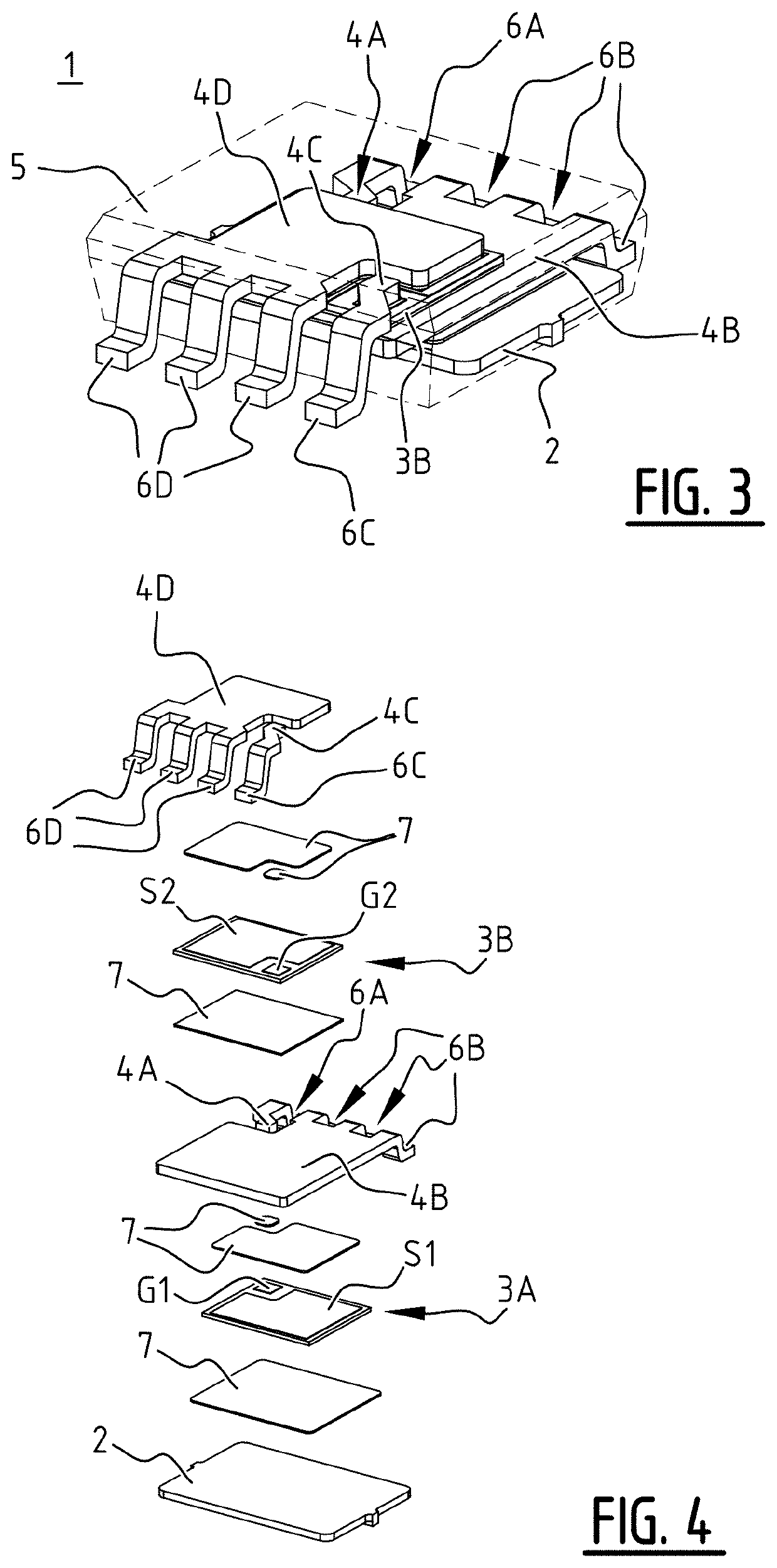
[0035]FIG. 3 shows a perspective view of a package 1 in accordance with an embodiment of the present disclosure, and FIG. 4 shows a corresponding exploded view of package 1.

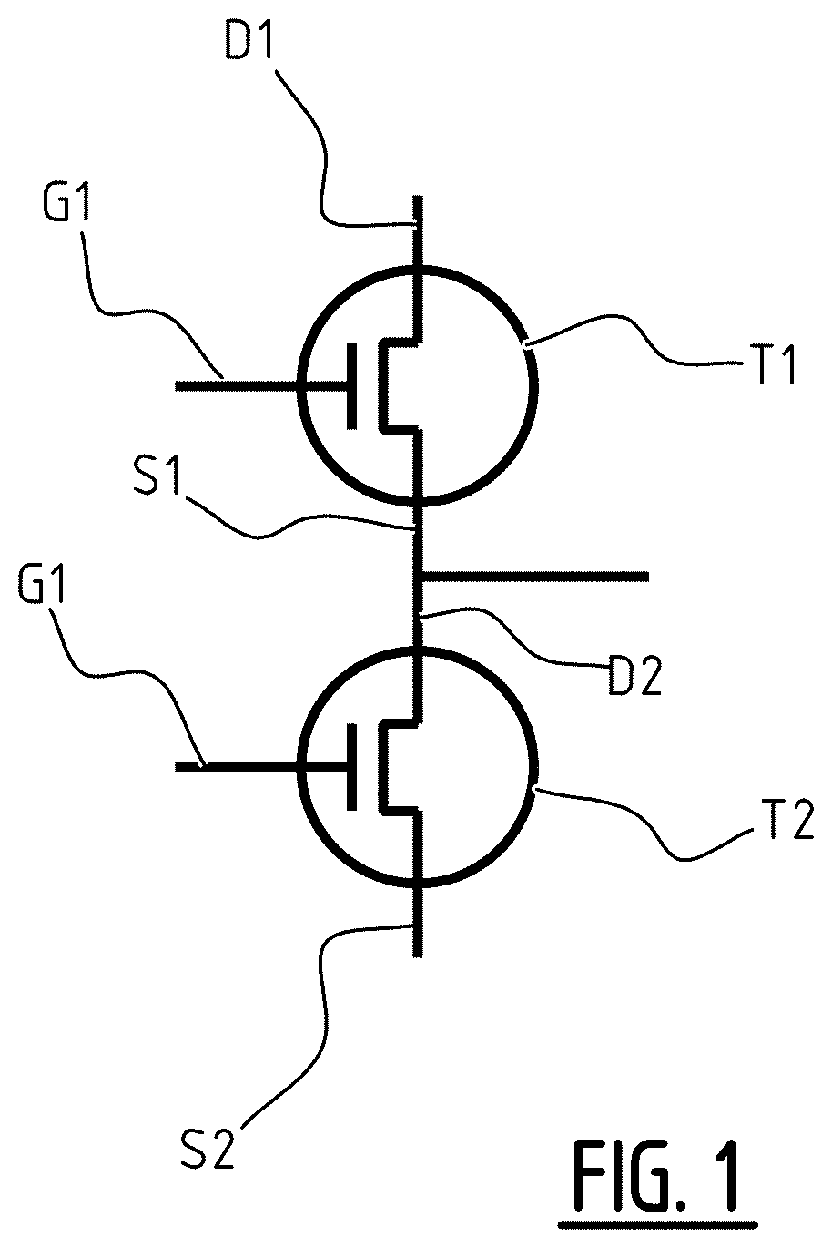
[0036]Package 1 comprises a die pad 2 having a first surface and a second surface. A first semiconductor die 3A (not visible in FIG. 3) is arranged on top of the first surface of die pad 2. First semiconductor die 3A has first transistor T1 integrated thereon. First transistor T1 comprises a first terminal G1 and a second terminal S1 arranged at a top surface of first semiconductor die 3A, and a third terminal D1 (not shown) arranged at a bottom surface of first semiconductor die 3A. Die pad 2 is electrically connected to third terminal D1 of first transistor T1 using a conductive layer, for example a solder or sinter layer 7, and may form a contact for said terminal.

[0037]Furthermore, package 1 comprises a first contact element 4A and a second contact element 4B that are arranged on top of first semiconductor di...


PUM


Abstract

A lead-frame based packaged half-bridge circuit is provided that is useful in power electronics applications, such as DC-DC converters and motor controllers. The circuit reduces or eliminates unwanted additional resistance and inductance produced from interconnections that degrade performance in typical packaged half-bridge circuits.

Description

CROSS REFERENCE TO RELATED APPLICATION[0001]This application claims the benefit under 35 U.S.C. § 119(a) of European Application No. 21162409.3 filed Mar. 12, 2021, the contents of which are incorporated by reference herein in their entirety.BACKGROUND OF THE DISCLOSURE1. Field of the Disclosure[0002]The present disclosure relates to a lead-frame based half-bridge package. The present disclosure is particularly useful in power electronics applications, such as DC-DC converters and motor controllers.2. Description of the Related Art[0003]A half-bridge circuit is an often used building block in various applications of power electronics, such as DC-DC converters or (H-bridge) motor controllers. For example, in a DC-DC converter, a half-bridge circuit may be used to control an output voltage of a transformer included in the DC-DC converter using two input switches included in the half-bridge circuit.[0004]An example of a half-bridge circuit is shown in FIG. 1. The half-bridge circuit co...

Claims


Application Information

Patent Timeline
Patent Type & Authority Applications(United States)
IPC IPC(8): H01L23/538H01L23/495H02P7/03H01L23/00
CPCH01L23/5381H01L23/49537H01L23/49575H01L23/49541H01L23/49568H02P7/04H01L24/29H01L2224/29099H01L23/4951H01L23/49517H01L23/31H01L23/49562H01L23/49524H01L2224/0603
Inventor YANDOC, RICARDO
Owner NEXPERIA BV
Why Eureka
Try Eureka