
Personal electronic device emp protective enclosure

a protective enclosure and electronic device technology, applied in the direction of electrical equipment, emergency protective arrangements for limiting excess voltage/current, transmission, etc., can solve the problems of emp-optimized nuclear devices, low yield detonation, fearsome threats, etc., to reduce radiation leakage path, enhance display clarity, prevent moiré patterns

Inactive Publication Date: 2022-09-22
SOFTRONICS
View PDF8 Cites 0 Cited by
  • Summary
  • Abstract
  • Description
  • Claims
  • Application Information

AI Technical Summary

Benefits of technology

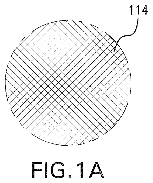
The patent text describes a mobile device case that has a top cover that has a special part that reduces harmful electromagnetic radiation while still allowing light to pass through. The special part is made of a thin metallic mesh that filters out everything but visible light. The case is designed to prevent interference with the display on the phone, making it clearer and easier to read. The case is also designed to reduce leaks of radiation.

Problems solved by technology

In particular, in the case of electronic equipment, EMP generates currents in microelectronic components, wires, printed circuit traces, etc., sufficient to vaporize or fuse those electronic elements, rendering them inoperative.
One of the most fearsome threats to the United States is detonation of a low yield, EMP-optimized nuclear device in low earth orbit (approx.
The resulting damage would be permanent, and leave the US with its industrial base also disabled and unable to repair or replace damaged electronics.
These are complex assemblies of miniature electronic components and interconnecting metal wires of various kinds, all of which are subject to damage by induced currents from a high-power EMP electromagnetic wavefront.
With the device installed inside of a sealed box with no openings, the device is obviously non-functional without a means for a user to physically or remotely access it.
While such cases may block a large portion of the EMF radiation from device while still allowing functionality for the user, having any radiation-transparent surface on the case leaves the mobile device susceptible to damage from an EMP.

Method used


Image

  • Personal electronic device emp protective enclosure
  • Personal electronic device emp protective enclosure
  • Personal electronic device emp protective enclosure

Examples


case 100

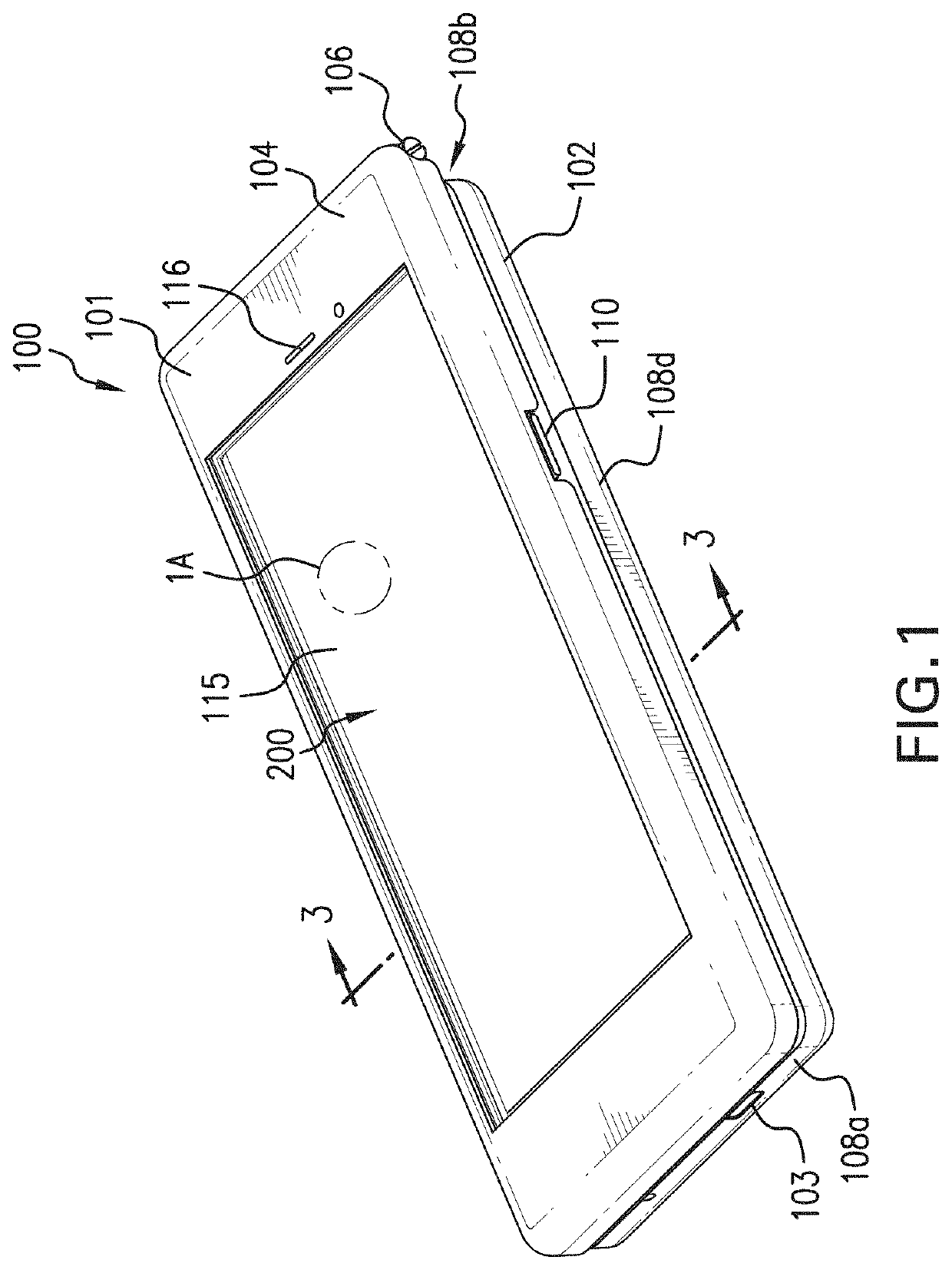
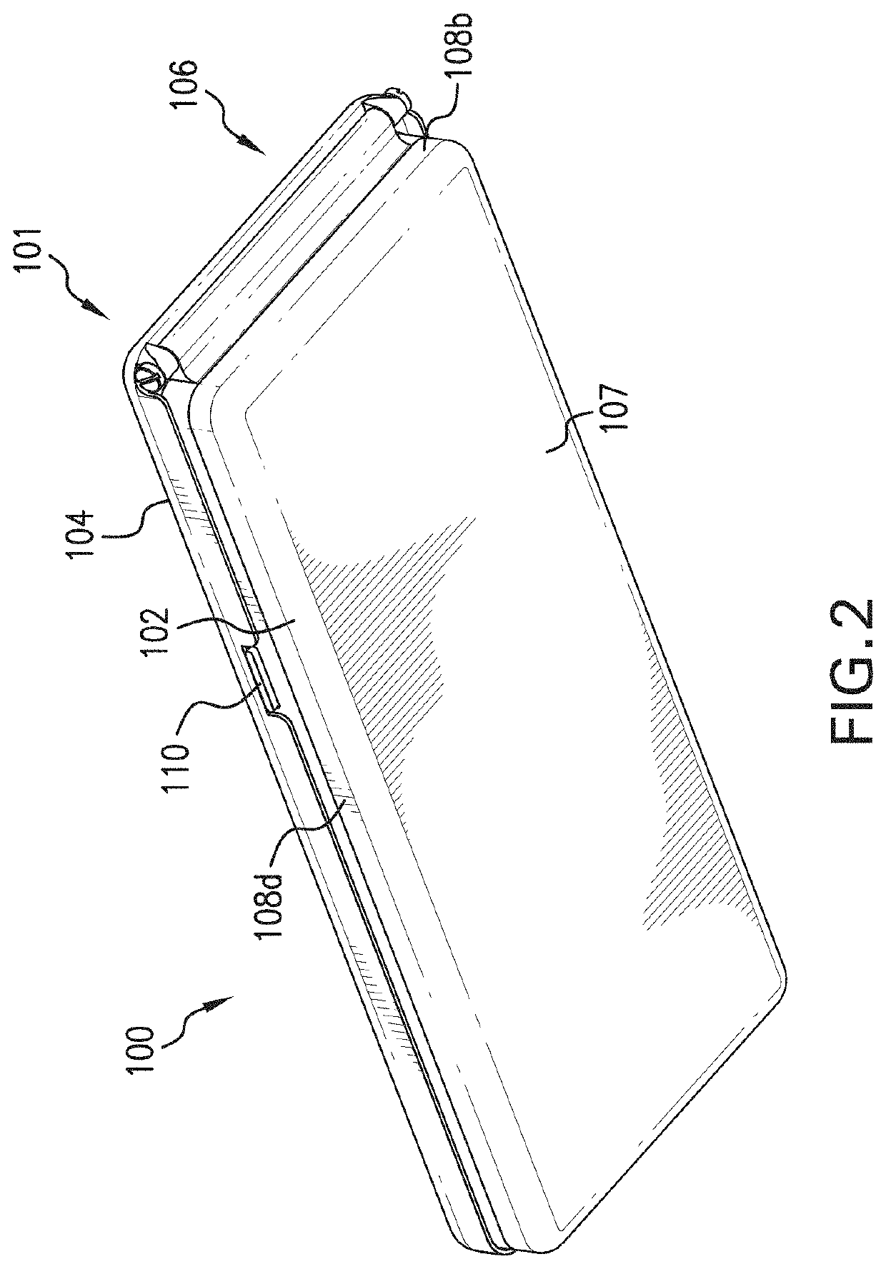
[0028]Case 100 comprises of an enclosure 101 with a hinged “visor” that completely surrounds mobile device 200. This hinged “visor” mechanically and electrically connected to the Faraday cage of enclosure 101 has a portion that aligns with the display where there is a cutout which fully reveals the display of mobile device 200. The cutout contains an optically-transmissive fine wire mesh which provides 80 db of radio attenuation. The mesh is sandwiched between two sheets of transparent plastic for damage and wear protection, with the mesh bonded to the grounded visor frame. Because the standard input entry touchscreen for mobile device 200 is capacitive, it will not function through a grounded mesh screen. Therefore, the user must open the visor to use the touchscreen of mobile device 200. Opening the visor, however, exposes mobile device 200 to EMP damage, requiring the user to take care where and when he opens it. This tradeoff recognizes that most use in emergency conditions is r...


PUM


Abstract

A Faraday cage enclosure for a mobile device with a portion that aligns with a display of the mobile device simultaneously substantially attenuate EM radiation to non-damaging amplitudes and is transparent to visible light in an optical spectrum, an EMP protection circuit electrically connected between the external charging and data port and the internal charging and data port, and a passive repeater configured to EM-couple with an antenna of the mobile device and relay signals to and from the antenna of the mobile device.

Description

PRIORITY CLAIM[0001]This application is a division of U.S. patent application Ser. No. 17 / 483,294 filed Jan. 23, 2021 which claims the benefit of U.S. Provisional Patent Application No. 63 / 162,298 filed on Mar. 17, 2021, the contents of which are hereby incorporated by reference herein.TECHNICAL FIELD[0002]The present invention relates generally to mobile cellular, wireless or Wi-Fi device accessories, and more particularly to a protective enclosure capable of protecting the device from an electro-magnetic pulse.BACKGROUND INFORMATION[0003]It is well understood that a high intensity electromagnetic wavefront generated by a nuclear detonation (or alternatively by special non-nuclear means) contains sufficient energy to induce destructive currents in conductive materials as it flows through and around them. Such a pulse is typically 100-200 nanoseconds in duration, with intensities on the order of 50 KV / m to 1 MV / m with the majority of energy concentrated in the 10-1000 MHz spectrum. ...

Claims


Application Information

Patent Timeline
Patent Type & Authority Applications(United States)
IPC IPC(8): H04B1/3888H02H9/04H01Q1/12H05K9/00
CPCH04B1/3888H02H9/04H01Q1/12H05K9/0081H05K9/0054H02H9/041H02H9/06
Inventor STERNOWSKI, ROBERT H.
Owner SOFTRONICS
Learn More