Power conversion module
- Summary
- Abstract
- Description
- Claims
- Application Information
AI Technical Summary
Benefits of technology
Problems solved by technology
Method used
Image

Examples
first embodiment
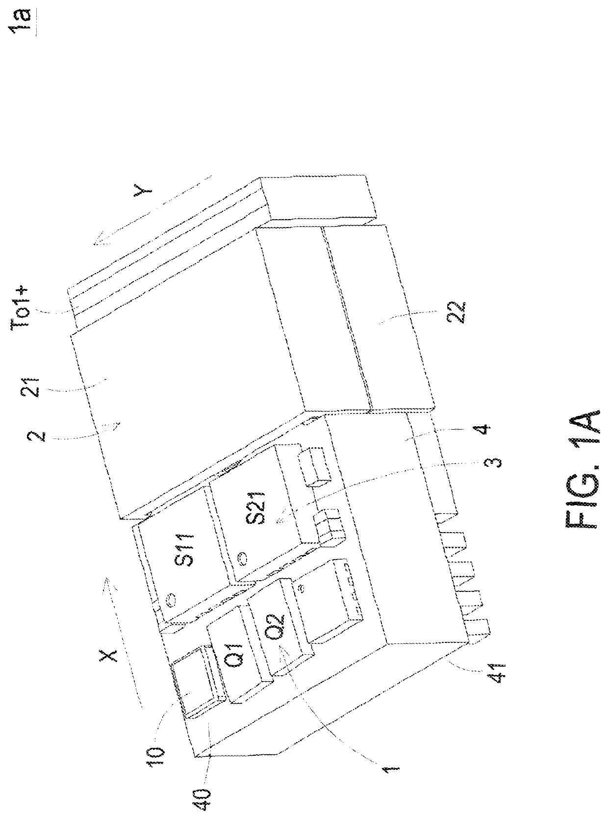
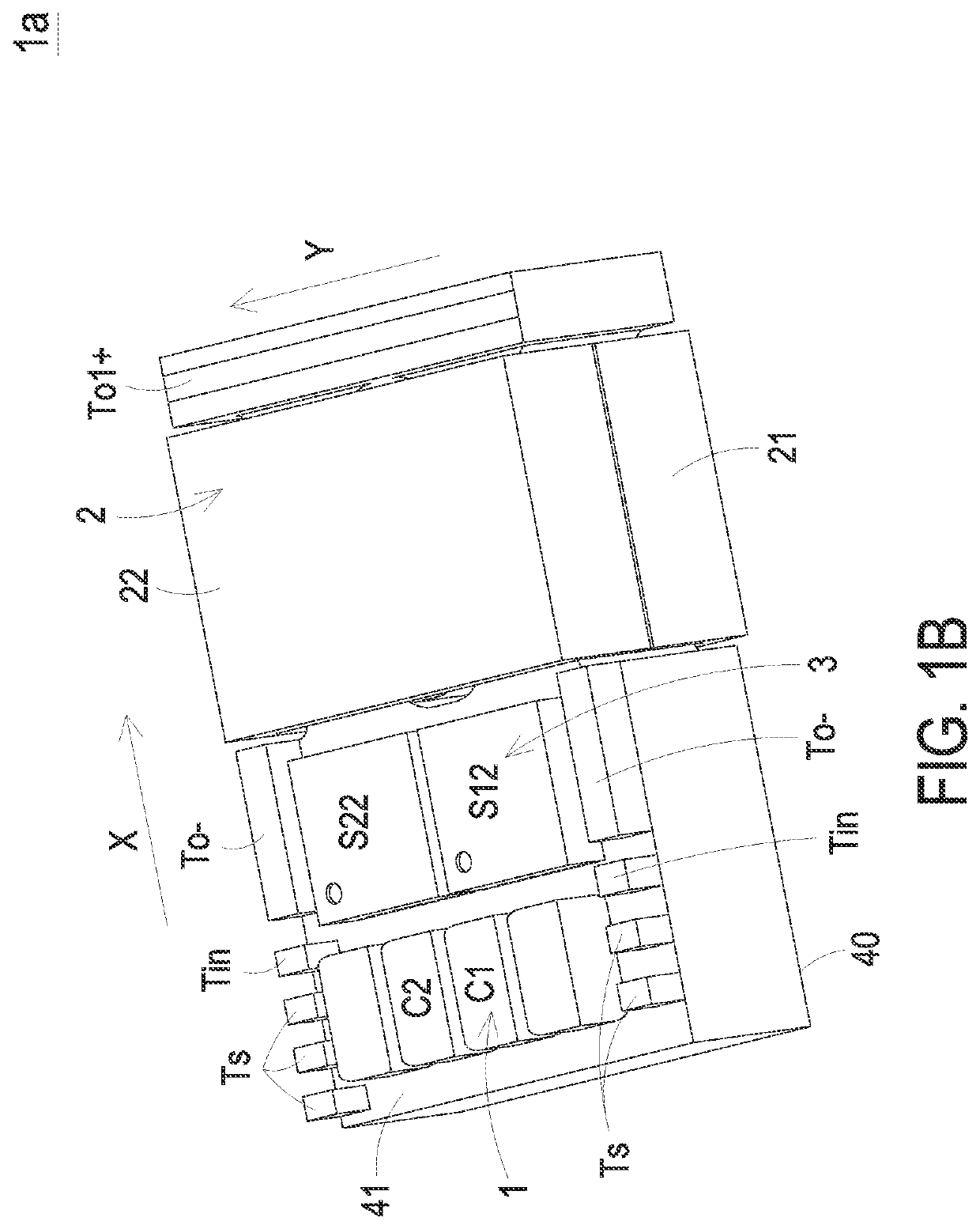
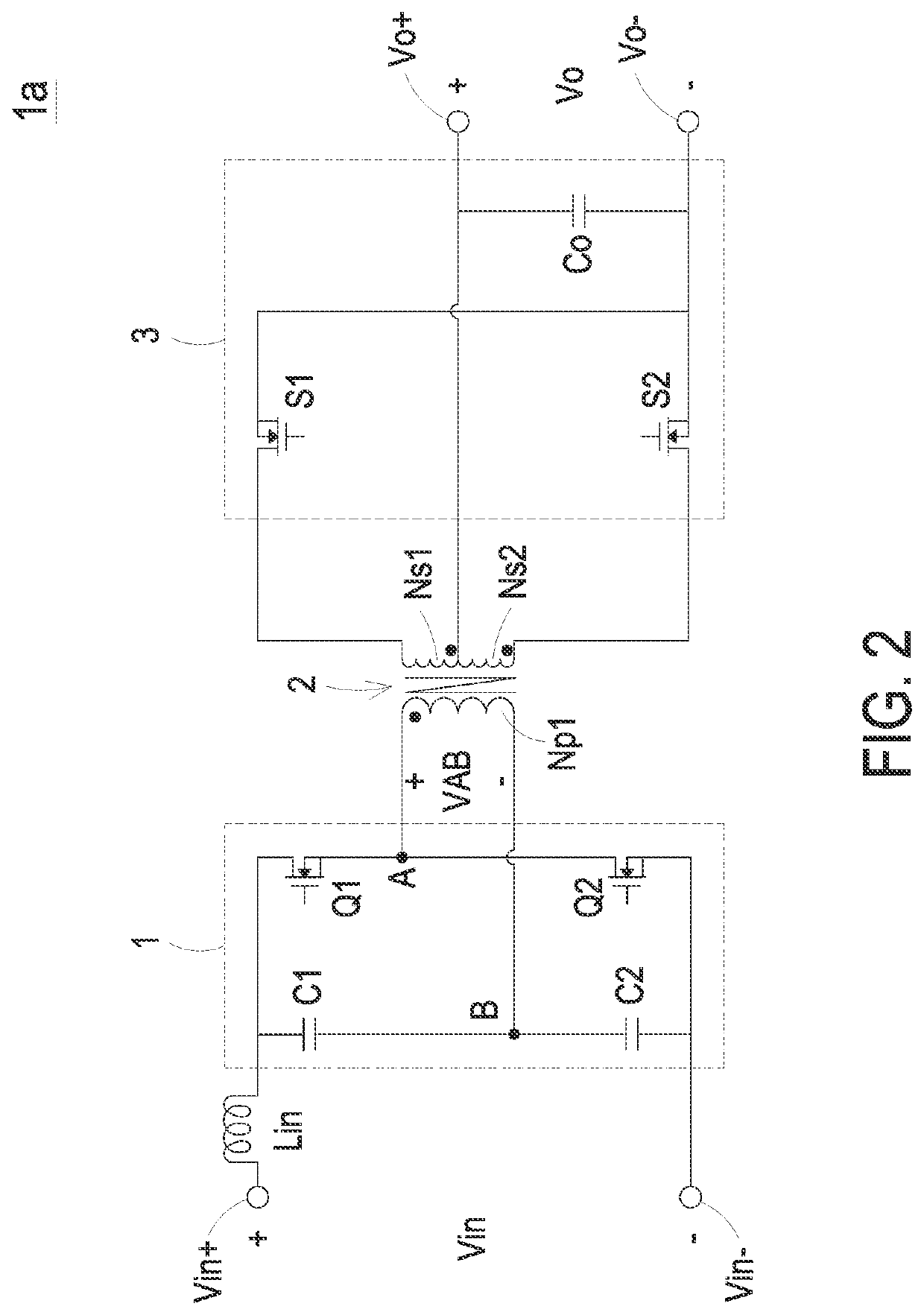
[0033]FIG. 1A is a schematic perspective view illustrating a power conversion module according to the present disclosure. FIG. 1B is a schematic perspective view illustrating the power conversion module as shown in FIG. 1A and taken along another viewpoint. FIG. 2 is a schematic circuit diagram illustrating the circuitry topology of the power conversion module as shown in FIG. 1A. FIG. 3 is a schematic timing waveform diagram illustrating the voltage signals of the power conversion module as shown in FIG. 1A. FIG. 4 is a schematic exploded view illustrating a magnetic core assembly of the magnetic device of the power conversion module as shown in FIG. 1A. FIG. 5 schematically illustrates the magnetic device of the power conversion module as shown in FIG. 1A, in which the first magnetic cover is omitted.
[0034]The circuitry topology of the power conversion module 1a of this embodiment is shown in FIG. 2, i.e., the power conversion module 1a is a single-stage conversion structure. The ...
third embodiment
[0082]FIG. 10A is a schematic perspective view illustrating a power conversion module according to the present disclosure. FIG. 10B is a schematic perspective view illustrating the power conversion module as shown in FIG. 10A and taken along another viewpoint. FIG. 10C is a schematic exploded view illustrating the power conversion module as shown in FIG. 10A. FIG. 11 schematically illustrates a variant example of the first magnetic device as shown in FIG. 10A, in which the first magnetic cover is omitted. In comparison with the power conversion module 1b, two magnetic devices 2b as shown in FIG. 9 are used in the power conversion module 1c of this embodiment to replace the first magnetic device 2 and the second magnetic device 2a as shown in FIG. 6A. Moreover, the first positive output terminal pin To1+ of the power conversion module 1c is disposed on at least one surface of the second magnetic cover 22 of the first magnetic device 2. For example, the first positive output terminal ...
fourth embodiment
[0085]FIG. 12 is a schematic circuit diagram illustrating the circuitry topology of a power conversion module according to the present disclosure. FIG. 13 schematically illustrates the magnetic device of the power conversion module as shown in FIG. 12, in which the first magnetic cover is omitted. In comparison with the power conversion module 1a of FIG. 2, the power conversion module 1d of this embodiment further includes an auxiliary winding Na. In addition, the structure of the magnetic device 2c in the power conversion module 1d of this embodiment is similar to that of the magnetic device 2b of FIG. 9. Component parts and elements corresponding to those of the above embodiments are designated by identical numeral references, and detailed descriptions thereof are omitted. The magnetic device 2c further includes the auxiliary winding Na. The auxiliary winding Na and the primary winding Np1 are magnetically coupled with each other. The auxiliary winding Na is further electrically c...
PUM
 Abstract
Description
Claims
Application Information
 - R&D
- Intellectual Property
- Life Sciences
- Materials
- Tech Scout
- Unparalleled Data Quality
- Higher Quality Content
- 60% Fewer Hallucinations
Browse by: Latest US Patents, China's latest patents, Technical Efficacy Thesaurus, Application Domain, Technology Topic, Popular Technical Reports.
© 2025 PatSnap. All rights reserved.Legal|Privacy policy|Modern Slavery Act Transparency Statement|Sitemap|About US| Contact US: help@patsnap.com