Detection Method for the Radiation-induced Defects of Oxide Layer in Electronic Devices

a technology of radiation-induced defects and electronic devices, which is applied in the direction of material analysis by transmitting radiation, etc., can solve the problems of affecting the property evolution of the electronic device, the quality and reliability of the electronic device directly affected by the electronic device, and the formation of radiation-induced defects of the oxide layer

Pending Publication Date: 2022-11-03
HARBIN INST OF TECH
View PDF0 Cites 0 Cited by
  • Summary
  • Abstract
  • Description
  • Claims
  • Application Information

AI Technical Summary

Problems solved by technology

In the semiconductor material, the migration rate of electrons does not differ from that of holes a lot, and therefore, great influences may not be caused when the radiation dosage is accumulated; however, in the oxide layer, the migration rate of electrons differs from that of holes a lot, the electrons formed by radiation will be migrated out of oxides, the remaining holes may be trapped by defects in the oxides in a transportation process, and thus, radiation-induced defects of the oxide layer are formed.
The oxygen vacancy defects may trap holes and may also trap electrons.
The oxide trapped charge in the electronic devices directly affects the quality and reliability of the electronic device.
Radiation-induced defects of the oxide layer are distributed in different states and may be positively charged or negatively charged, and these features may affect property evolution of the electronic device.
An existing micro-analysis means for detecting the states of the defects in the semiconductor material is relatively low in sensitivity and incapable of checking and analyzing radiation-induced defects of the oxide layer, and therefore, how to rapidly, efficiently and accurately detect the states of radiation-induced defects of the oxide layer in the electronic devices becomes a problem to be solved urgently at present.

Method used


Image

  • Detection Method for the Radiation-induced Defects of Oxide Layer in Electronic Devices
  • Detection Method for the Radiation-induced Defects of Oxide Layer in Electronic Devices
  • Detection Method for the Radiation-induced Defects of Oxide Layer in Electronic Devices

Examples


first embodiment

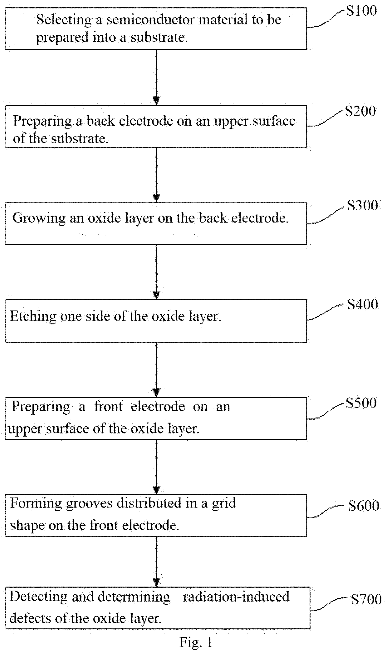
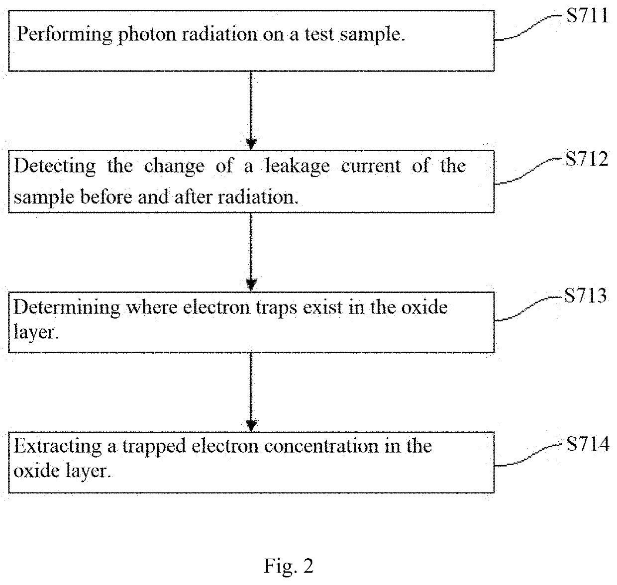
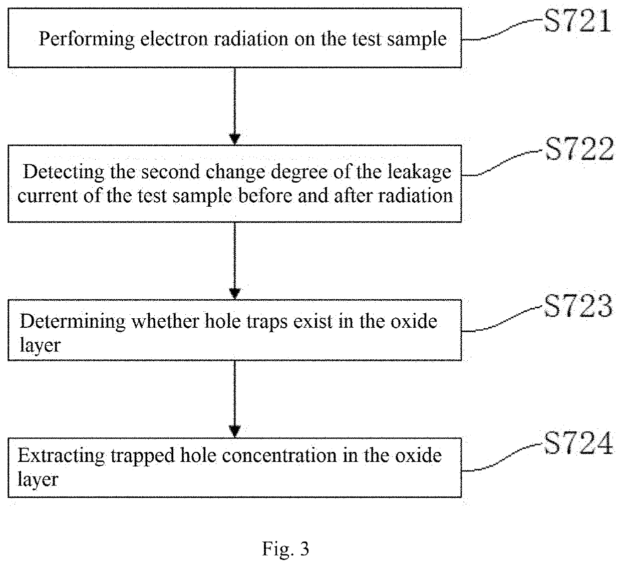
[0065]The present embodiment provides a detection method for radiation-induced defects of an oxide layer in electronic devices. As shown in FIG. 4 and FIG. 5, the detection method includes the following steps.

[0066]Step S100: an N-type semiconductor material is selected to be prepared into a substrate 1, wherein the doping concentration of the substrate 1 is 1e19 cm−3, the thickness ti of the substrate 1 is 50 mm, and the substrate is square and has the area of 10 mm×10 mm.

[0067]Step S200: a back electrode 2 is prepared on an upper surface of the substrate 1 by physical vapor deposition.

[0068]Step S300: an oxide layer is prepared on the back electrode 2 in a dry / wet oxygen mixed manner. Specifically, firstly, dry oxygen oxidation is performed for 30 min, then, wet oxygen oxidation is performed for 60 min, and finally, dry oxygen oxidation is performed for 50 min. The manner is the same as an oxidation manner of a to-be-tested electronic device.

[0069]Step S400: one side of the oxide ...

second embodiment

[0082]The present embodiment provides a detection method for radiation-induced defects of an oxide layer in electronic devices. The detection method includes the following steps.

[0083]Step S100: a P-type semiconductor material is selected to be prepared into a substrate, wherein the doping concentration of the substrate is 1e20 cm−3, the thickness of the substrate is 1 mm, and the substrate is square and has the area of 1 mm×1 mm.

[0084]Step S200: a back electrode is prepared on an upper surface of the substrate by chemical vapor deposition.

[0085]Step S300: an oxide layer is prepared on the back electrode in a dry oxygen manner. Specifically, dry oxygen oxidation is performed for 80 min. The manner is the same as an oxidation manner of a to-be-tested electronic device.

[0086]Step S400: one side of the oxide layer is etched, wherein the etching area is 100 μm×100 μm and wet etching is adopted as an etching manner; and an etched part is exposed out of the back electrode.

[0087]Step S500:...

third embodiment

[0099]The present embodiment provides a detection method for radiation-induced defects of an oxide layer in electronic devices. The detection method includes the following steps.

[0100]Step S100: an N-type semiconductor material is selected to be prepared into a substrate, wherein the doping concentration of the substrate is 1e21 cm−3, the thickness of the substrate is 100 mm, and the substrate is rectangular and has the area of 1 mm×2 mm.

[0101]Step S200: a back electrode is prepared on an upper surface of the substrate by gold metallization.

[0102]Step S300: an oxide layer is prepared on the back electrode in a wet oxygen manner. Specifically, wet oxygen oxidation is performed for 90 min. The manner is the same as an oxidation manner of a to-be-tested electronic device.

[0103]Step S400: one side of the oxide layer is etched, wherein the etching area is 0.5 mm×1 mm, and plasma etching is adopted as an etching manner; and an etched part is exposed out of the back electrode.

[0104]Step S5...


PUM

PropertyMeasurementUnit
resistivityaaaaaaaaaa
energyaaaaaaaaaa
electric fieldaaaaaaaaaa

Abstract

The present invention provides a detection method for radiation-induced defects of an oxide layer in electronic devices. The detection method includes the following steps: selecting a semiconductor material to be prepared into a substrate; preparing a back electrode on an upper surface of the substrate; growing an oxide layer on the back electrode; etching one side of the oxide layer, and exposing an etched part out of the back electrode; preparing a front electrode on an upper surface of the oxide layer; forming a plurality of grooves in the front electrode, and distributing the plurality of grooves in a grid shape to prepare a test sample; and performing a radiation test on the test sample, and detecting radiation-induced defects. By using the detection method provided by the present invention, rapid identification and detection of electrons and holes are achieved.

Description

TECHNICAL FIELD[0001]The present invention relates to the technical field of electronic devices, in particular to, a detection method for radiation-induced defects of an oxide layer in electronic devices.BACKGROUND ART[0002]When an electronic device is radiated, electron-hole pairs may be generated in a semiconductor material and an oxide layer in the electronic devices, most of these electron-hole pairs may be initially combined, and the remaining electron-hole pairs will be diffused or drifted away under the action of a concentration gradient or electric field. In the semiconductor material, the migration rate of electrons does not differ from that of holes a lot, and therefore, great influences may not be caused when the radiation dosage is accumulated; however, in the oxide layer, the migration rate of electrons differs from that of holes a lot, the electrons formed by radiation will be migrated out of oxides, the remaining holes may be trapped by defects in the oxides in a tran...

Claims


Application Information

Patent Timeline
Patent Type & Authority Applications(United States)
IPC IPC(8): G01N23/18
CPCG01N23/18G01N23/02
Inventor LI, XINGJIYANG, JIANQUNXU, XIAODONGLV, GANGCUI, XIUHAIYING, TAOWEI, YADONG
Owner HARBIN INST OF TECH
Why Eureka
Try Eureka