

Semiconductor apparatus and semiconductor apparatus manufacturing method
- Summary
- Abstract
- Description
- Claims
- Application Information
AI Technical Summary
Benefits of technology
Problems solved by technology
Method used
Image

Examples
first embodiment
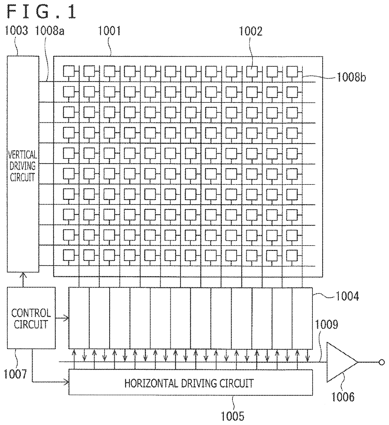
[0113]As a semiconductor apparatus according to a first embodiment of the present technology, a backside illumination CMOS image sensor (solid-state image pickup apparatus) is illustrated. As depicted in FIG. 1, the semiconductor apparatus according to the first embodiment of the present technology includes a pixel region (unit cell region) 1001, a vertical driving circuit 1003, column signal processing circuits 1004, a horizontal driving circuit 1005, an output circuit 1006 and a control circuit 1007.
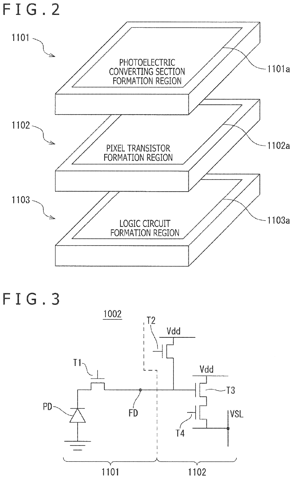
[0114]The pixel region 1001 has plural pixels (unit cells) 1002 arrayed in a two-dimensional matrix. Each of the plural pixels 1002 has a photoelectric converting section and plural pixel transistors (cell circuits). As the plural pixel transistors, for example, four transistors which are a transfer transistor, a reset transistor, a selection transistor and an amplification transistor can be adopted.
[0115]For example, the vertical driving circuit 1003 includes a shift register. The ver...
modification example of first embodiment
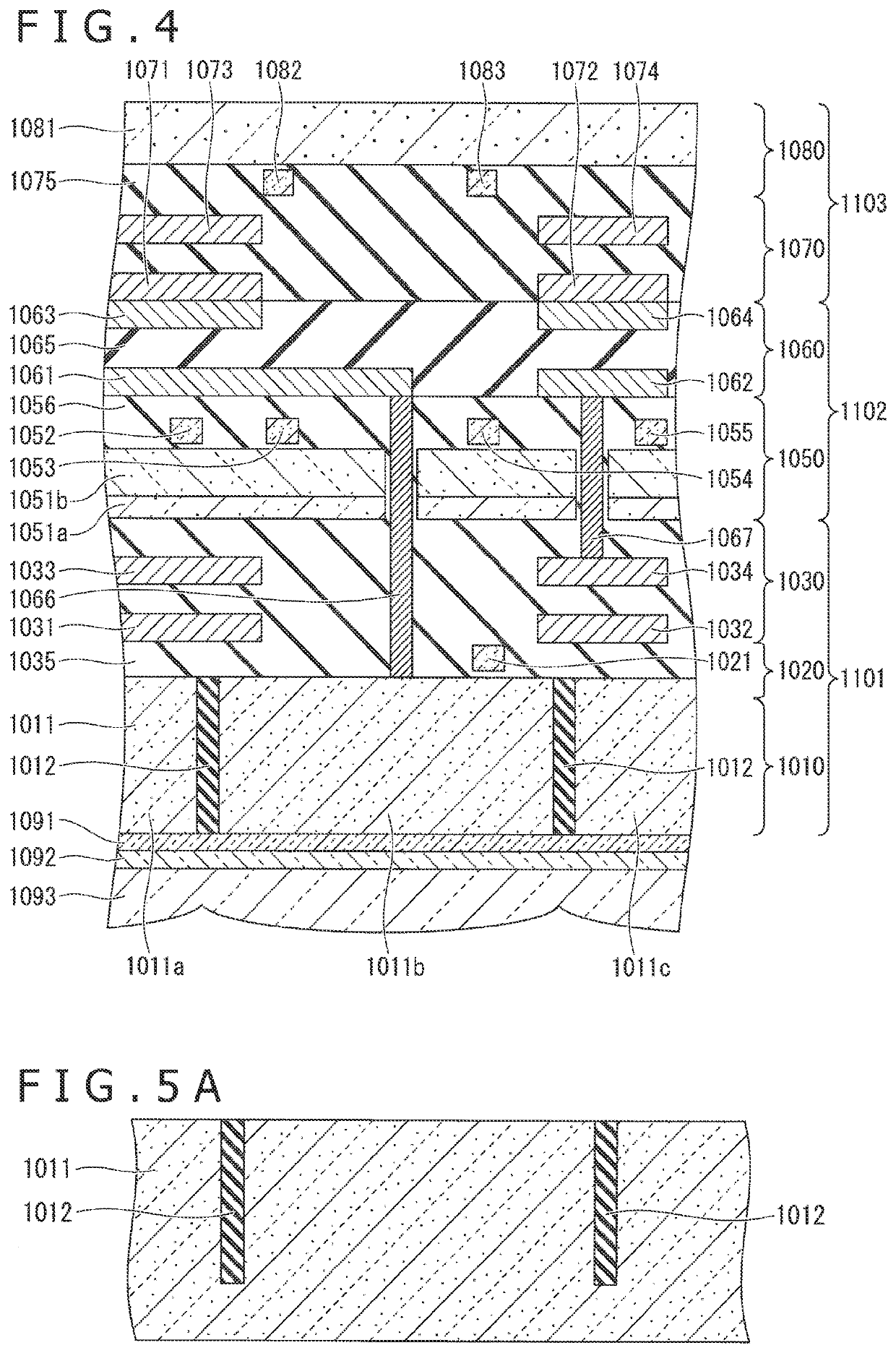
[0162]As depicted in FIG. 11, a semiconductor apparatus according to a modification example of the first embodiment of the present technology is different from the semiconductor apparatus according to the first embodiment of the present technology depicted in FIG. 4 in that the second element layer 1050 does not have the Si substrate 1051a, but includes a single layer of the semiconductor substrate (compound semiconductor substrate) 1051b including a compound semiconductor. In other respects, the configuration of the semiconductor apparatus according to the modification example of the first embodiment of the present technology is similar to that of the semiconductor apparatus according to the first embodiment of the present technology depicted in FIG. 4, and so overlapping explanations are omitted.
[0163]According to the semiconductor apparatus according to the modification example of the first embodiment of the present technology, because the second element layer 1050 has the second...
second embodiment
[0165]The semiconductor apparatus according to a second embodiment of the present technology can be applied to a solid-state image pickup apparatus or the like similarly to the semiconductor apparatus according to the first embodiment of the present technology. The overall configuration of the semiconductor apparatus according to the second embodiment of the present technology is similar to the overall configuration of the semiconductor apparatus according to the first embodiment of the present technology depicted in FIG. 1, and so overlapping explanations are omitted.
[0166]FIG. 12 schematically depicts a part of the cross-sectional structure of the semiconductor apparatus according to the second embodiment. The semiconductor apparatus according to the second embodiment has a stacked structure formed by pasting and joining together three substrates which are a first substrate 2101, a second substrate 2102 and a third substrate 2103. The semiconductor apparatus according to the secon...
PUM
 Abstract
Description
Claims
Application Information