Silicon-on-insulator-device and fabrication method thereof

a technology of silicon-on-insulator substrate and mosfet structure, which is applied in the direction of semiconductor devices, electrical devices, transistors, etc., can solve the problems of parasitic effects, low silicon-on-insulator performance, and difficult implementation of the effect of mosfet structure in the field of silicon-on-insulator substrate fabrication

Inactive Publication Date: 2000-02-29
LG SEMICON CO LTD
View PDF1 Cites 44 Cited by
  • Summary
  • Abstract
  • Description
  • Claims
  • Application Information

AI Technical Summary

Problems solved by technology

The performance of thin-film MOSFETs suffer, however, from parasitic effects, notably high sheet resistance of and high contact resistance to the thin film source / drain regions.
In addition, MOSFET structures fabricated on silicon-on-insulator substrates are subject to floating-body effects, which occur because the body of the active (device) region of the silicon-on-insulator substrate (ie., the region of the substrate above the buried oxide layer) is not easily held at a constant potential, in contrast to the body of a bulk single-crystal silicon substrate (i.e., a substrate without a buried oxide layer), the back surface of which can easily be grounded.
Notwithstanding the several advantages of the silicon-on-insulator MOSFET structure of Hieda, et al. seen in simulation, such advantages would not easily be realized in practice, since the structure would be very difficult to fabricate.

Method used


Image

  • Silicon-on-insulator-device and fabrication method thereof
  • Silicon-on-insulator-device and fabrication method thereof
  • Silicon-on-insulator-device and fabrication method thereof

Examples


Embodiment Construction

EMBODIM9IENTS

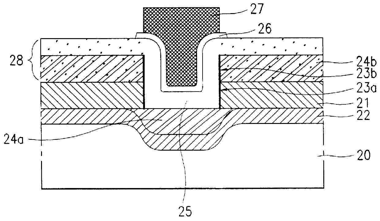
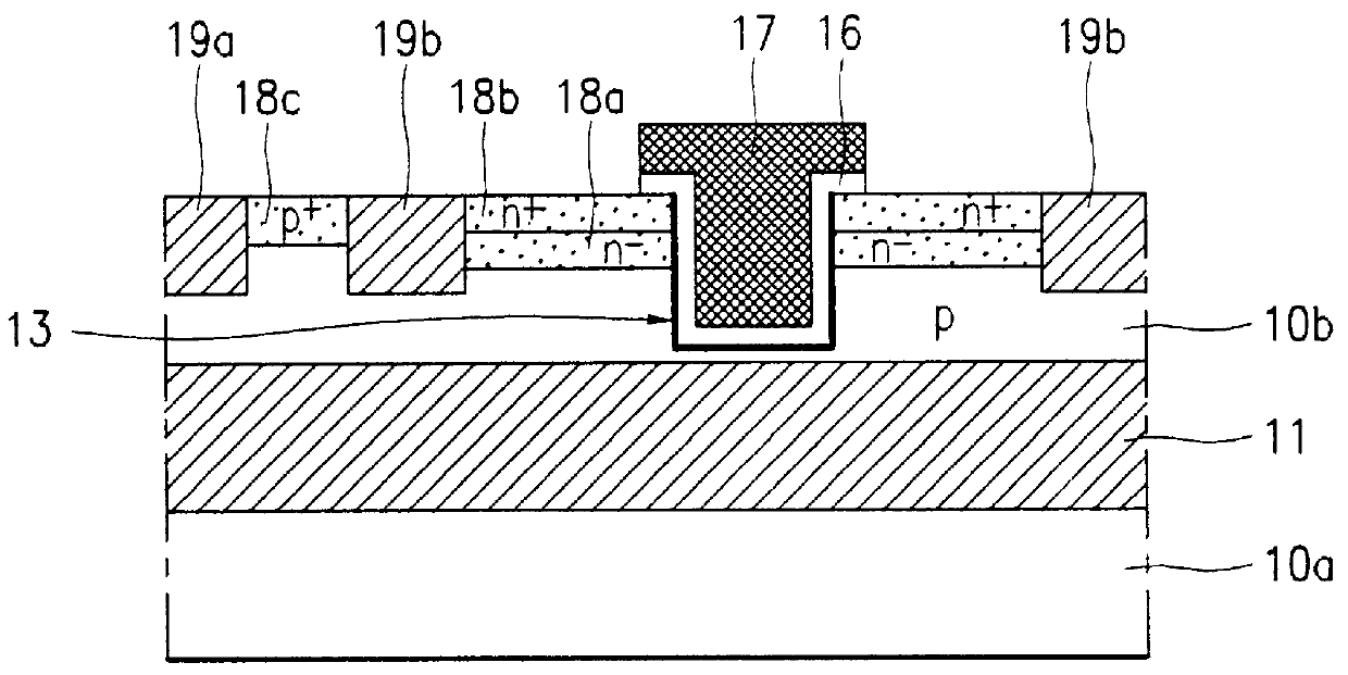
As shown in the idealized cross-sectional view of FIG. 2, the silicon-on-insulator MOSFET of the present invention includes:

a silicon substrate 20;

a continuous, substantially planar first buried insulating layer 21 within the substrate, which first buried layer preferably consists of either silicon dioxide (SiO.sub.2) or silicon nitride (Si.sub.3 N.sub.4) and defines an upper region 20b of the substrate above the first buried layer (hereinafter referred to as the upper substrate 20b) and a lower region 20a of the substrate below the first buried layer (hereinafter referred to as the lower substrate 20a), where the upper substrate has a hole 23b and the first buried layer has a hole 23a substantially aligined with the hole through the upper substrate;

a lower doped reuion 24a of a first conductivity type within the lower substrate 20a below the hole 23a through the first buried layer;

a continuous second buried insulating layer 22 within the lower substrate 20a, which seco...


PUM


Abstract

A two-layer buried oxide enables fabrication of a silicon-on-insulator MOSFET with thick-film source/drain regions and a thin-film channel region. After a hole has been etched in the substrate above a first buried oxide layer (i.e., in the upper substrate), oxygen is implanted to form a second buried layer within the substrate below the first buried layer (i.e., within the lower substrate). After a hole (aligned with the hole through the upper substrate) has been etched in the first buried layer, p-type dopants are implanted to form upper doped regions within the upper substrate to either side of the holes and a lower doped region within the lower substrate below the holes but above the second buried layer. An epitaxial layer roughly as thick as first buried layer is grown on the upper and lower substrates, a conformal insulating film is deposited onto the epitaxial layer, and a gate electrode is formed on the on the insulating film. Implantation of n-type dopants into both the epitaxial layer and the upper substrate to either side of the holes completes fabrication of the silicon-on-insulator device.

Description

1. Field of the InventionThe present invention relates to a silicon-on-insulator semiconductor device and, more particularly, to an silicon-on-insulator metal-oxide-semiconductor field effect transistor (MOSFET) and also to a method of fabricating the device.2. Discussion of the Related ArtThe term silicon-on-insulator collectively refers to device isolation technologies through which a device fabricated on a silicon substrate is electrically isolated from other devices on the substrate by means of an insulating region bordering the device. Although the origin of silicon-on-insulator technologies may be traced back to a 1934 German patent issued to Oscar Heil, silicon-on-insulator substrates escaped categorization as exotic materials only in the 1980's and were introduced into high-volume production for a limited range of applications only in the early 1990's. Of the many processes that were proposed during the 1980's for fabricating thin-film silicon-on-insulator structures, only S...

Claims


Application Information

Patent Timeline
Patent Type & Authority Patents(United States)
IPC IPC(8): H01L21/70H01L21/266H01L21/336H01L29/423H01L21/762H01L29/40H01L21/02H01L29/786H01L29/66H01L21/265
CPCH01L21/266H01L21/76264H01L29/66772H01L29/78654H01L29/78696H01L21/26533H01L21/76267H01L29/66651H01L21/76224H01L21/823857H01L21/823892H01L29/4236H01L29/66621
Inventor KANG, CHANG YONG
Owner LG SEMICON CO LTD
Why Eureka
Try Eureka