
Incremental critical area computation for VLSI yield prediction

a critical area and computation technology, applied in the direction of semiconductor/solid-state device testing/measurement, instruments, semiconductor devices, etc., can solve the problems of open circuit, defects caused by fabrication defects, and defects that are caused by via blocks and breaks

Inactive Publication Date: 2000-03-28
GLOBALFOUNDRIES INC
View PDF8 Cites 42 Cited by
  • Summary
  • Abstract
  • Description
  • Claims
  • Application Information

AI Technical Summary

Problems solved by technology

Fabrication defects are caused by contaminants in materials and equipment.
Essentially, there are two types of contamination caused manufacturing defects: extra material, causing shorts between different conducting regions and missing material, causing open circuits.
Because of missing material we get two kinds of defects: breaks and via blocks.
Via blocks are missing material defects that overlap with vias and thus destroy the connection between elements of the same net in different layers.

Method used


Image

  • Incremental critical area computation for VLSI yield prediction
  • Incremental critical area computation for VLSI yield prediction
  • Incremental critical area computation for VLSI yield prediction

Examples


Embodiment Construction

The L.sub..infin. Metric

In the state of the art defect modeling techniques, defects are modeled, consistently, as circles. The underlying reason for modeling defects as circles is the common use of Euclidean geometry. Distance between two points, typically, is measured by the length of a line segment joining the two points. This is the Euclidean distance or the L.sub.2 metric. The locus of points at unit distance from a center point is usually called the "unit circle". In Euclidean geometry, the "unit circle" is a circle of radius one.

In reality, defects need not be circular. In fact they can have any shape. Thus, as the inventors of the present invention have found, other than the Euclidean geometries, although not normally used, may be used and simplify the computation of critical area. See also U.S. application Ser. No. 09 / 085,093, (Attorney Docket Number YO9-97-223).

Therefore, according to the preferred embodiment of the present invention, critical area is computed in the L.sub....


PUM


Abstract

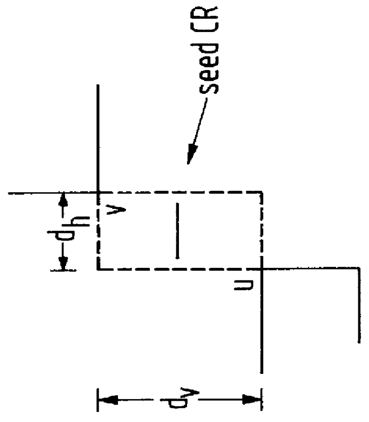
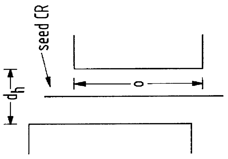
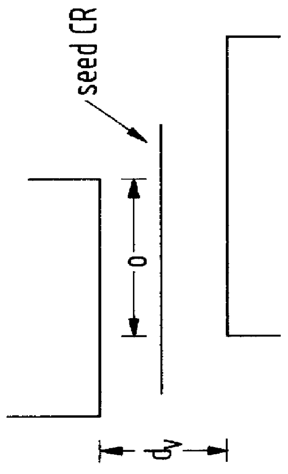
An efficient method to compute critical area for shorts and breaks in rectilinear layouts in Very Large Scale Integrated (VLSI) circuits. The method is incremental and works in the L INFINITY geometry and has three major steps: Compute critical area for rectilinear layouts for both extra material and missing material defects (i.e., shorts and opens) by modeling defects as squares (which corresponds to the L INFINITY metric) instead of circles (Euclidean geometry). Treat the critical region for shorts and opens between any two edges or corners of the layout as a rectangle that grows uniformly as the defect radius increases. This is valid for rectilinear layouts and square defects (L INFINITY metric) . Use an incremental critical area algorithm for shorts and opens, which are computed for rectilinear layouts assuming square defects. Non-rectilinear layouts are approximated, first, by a rectilinear layout using a shape processing tool. The critical area for the rectilinear approximation is computed using the preferred incremental method.

Description

DESCRIPTION1. Field of the InventionThe present invention generally relates to yield estimation techniques for large complex circuit designs and, more particularly, to an incremental method for critical area computation of shorts and opens in very large scale integrated (VLSI) circuits.2. Description of the Prior ArtYield prediction is of growing importance in modern VLSI design due to the need for reducing the cost of manufacturing. Yield estimation techniques for large complex designs are based on the concept of critical area which provides an analytical formulation for yield loss caused by defects occurring during fabrication.For examples of state of the art yield prediction techniques, see, W. Maly and J. Deszczka, "Yield Estimation Model for VLSI Artwork Evaluation", Electron Lett., vol. 19, no. 6, pp. 226-227, March 1983, C. H. Stapper, "Modeling of defects in integrated circuits photolithographic patterns", IBM J. Research and Development, vol. 28, no. 4, pp. 461-475, 1984, W...

Claims


Application Information

Patent Timeline
IPC IPC(8): H01L21/66
CPCH01L22/20H01L2924/0002H01L2924/00
Inventor PAPADOPOULOU, EVANTHIALAVIN, MARK ALAN
Owner GLOBALFOUNDRIES INC
Learn More