Eureka AIR delivers breakthrough ideas for toughest innovation challenges, trusted by R&D personnel around the world.

System and method for model size reduction of an integrated circuit utilizing net invariants

a technology of net invariants and integrated circuits, applied in the direction of instruments, analogue processes for specific applications, electric/magnetic computing, etc., can solve the problems of reducing the simulation speed of integrated circuits, and affecting the simulation efficiency of integrated circuits. , to achieve the effect of reducing the amount of integrated circuits, reducing space, and increasing the simulation speed

Inactive Publication Date: 2000-04-11
IBM CORP
View PDF20 Cites 12 Cited by
  • Summary
  • Abstract
  • Description
  • Claims
  • Application Information

AI Technical Summary

Benefits of technology

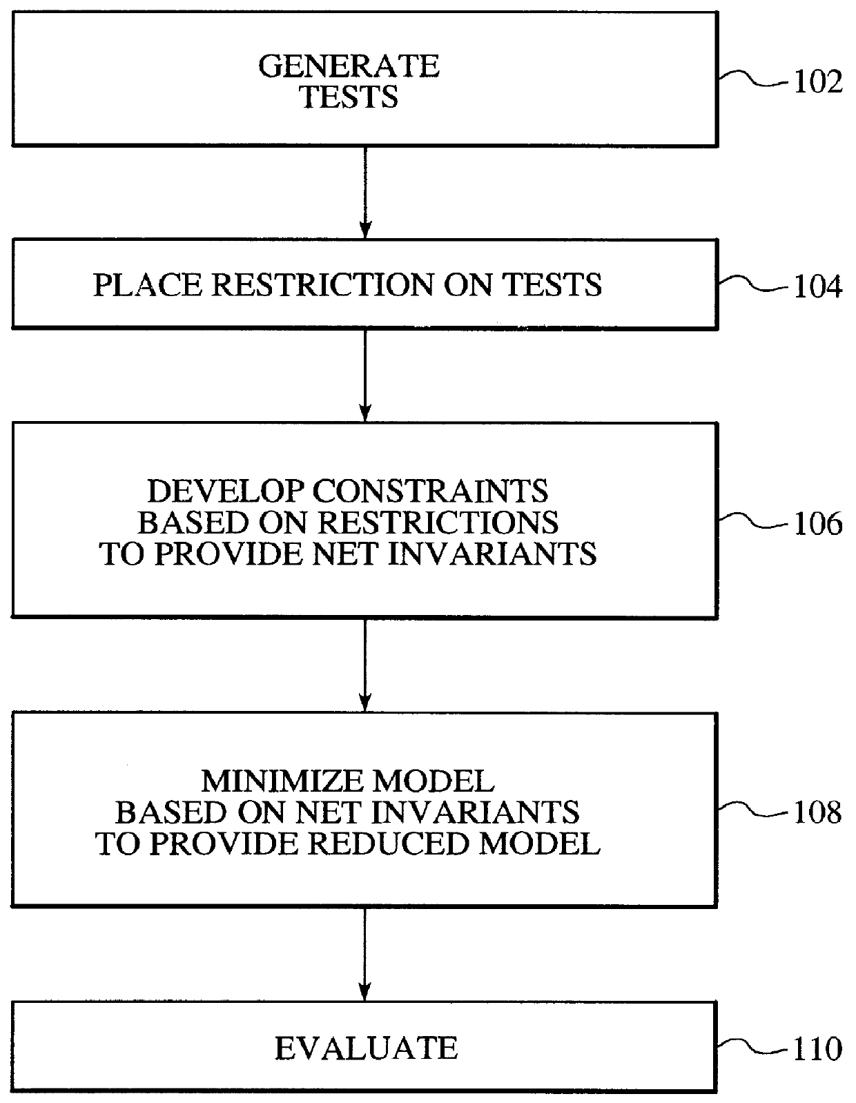
In a preferred embodiment, the present invention includes restricting the tests that are generated. Then net invariants for the integrated circuit are generated by translating the restricted tests to a smaller set of possible values for the net variables. Note that a smaller set of possibilities for net variables can occur naturally and not strictly from test restrictions. Thereafter, a minimization algorithm or procedure is utilized to minimize the logic used in the particular system based upon the reduced set of values for the net variables. This system produces a reduced model which reduces the amount of the integrated circuit that must be simulated thereby increasing the simulation speed thereof. Accordingly, the present invention integrates an event-driven simulation and a cycle simulation in such a manner that the saving can be proportional to the size of the reduction of the model. In many environments this reduction is significant because it allows for a significant reduction in space which has a clear bearing on the verification process.

Problems solved by technology

Typically, simulation and / or emulation of an integrated circuit is relatively expensive and time consuming.
Model sizes pose severe restrictions on every form of verification be it simulation, emulation, or formal verification.
In the case of large multi-processor systems, it may take months to simulate the design for all the planned test programs on a set of resources.
In some instances pre-silicon verification efforts are abandoned simply because the model size was too large for the resources to handle.
Escalating complexity of modern digital designs is destined to make these problems even more acute.
However, to evaluate all gates for each cycle as is required in cycle simulators becomes very time consuming and expensive.
This is particularly true, in complex designs such as multiprocessing architectures and the like.

Method used


Image

  • System and method for model size reduction of an integrated circuit utilizing net invariants
  • System and method for model size reduction of an integrated circuit utilizing net invariants

Examples


Embodiment Construction

The present invention is directed toward an improvement in simulation of integrated circuits. The following description is presented to enable one of ordinary skill in the art to make and use the illustrative embodiment and is provided in the context of a patent application and its requirements. Various modifications to the illustrative embodiment will be readily apparent to those skilled in the art and the generic principles herein may be applied to other embodiments. Thus, the illustrative embodiment is not intended to be limited to the embodiment shown but is to be accorded the widest scope consistent with the principles and features described herein.

An integrated circuit model (M) can be represented by:

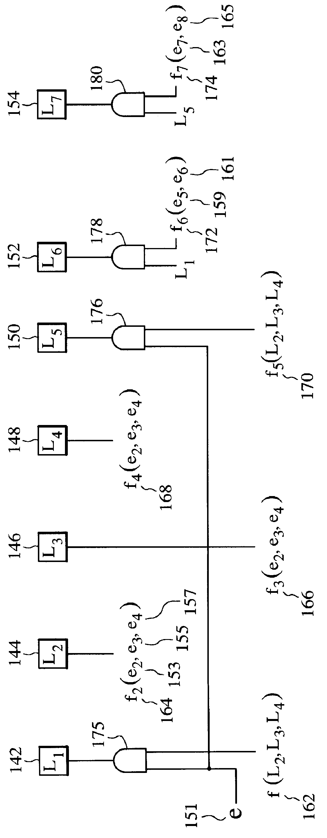
where L is a complete set of net variables and f.sub.i is the set of boolean functions of the corresponding set of net variables in terms of other net variables, external variables and outputs. In most emulation platforms there is a desire to reduce the size of the integrated circ...


PUM


Abstract

The present invention provides a system and method for verifying an integrated circuit model. The model includes a plurality of net variables. The system and method comprises generating a plurality of tests for simulating the integrated circuit, precalculating a reduced model based upon the generated tests, and evaluating the reduced model. In a preferred embodiment, the present invention includes restricting the test that are generated. Then net invariants for the integrated circuit are generated by translating the restricted plurality of tests to a smaller set of possible values for the net variables. Thereafter, a minimization algorithm or procedure is utilized to minimize the logic used in the particular system based upon the latch constraints. This system produces a reduced model which reduces the amount of the integrated circuit that must be simulated thereby increasing the simulation speed thereof. Accordingly, the present invention integrates an event-driven simulation and a cycle simulation in such a manner that the saving can be proportional to the size of the reduction of the model. In many environments this reduction is significant because it allows for a significant reduction in space which has a clear bearing on the verification process.

Description

TECHNICAL FIELDThe present invention is related to simulation and / or emulation of integrated circuits, and more particularly to a system and method for reducing the size of such for simulation, emulation or for other purposes.BACKGROUNDSimulation and / or emulation of an integrated circuit is a primary vehicle for design verification of an integrated circuit, particularly one that includes random logic. Typically, simulation and / or emulation of an integrated circuit is relatively expensive and time consuming. Model sizes pose severe restrictions on every form of verification be it simulation, emulation, or formal verification. For instance, simulation resource requirements are a function of the model size. In the case of large multi-processor systems, it may take months to simulate the design for all the planned test programs on a set of resources. If the model size is reduced by half then the time or the resource requirement is also reduced by 50%. This translates to significant doll...

Claims


Application Information

Patent Timeline
Patent Type & Authority Patents(United States)
IPC IPC(8): G01R31/317G01R31/28G06F17/50
CPCG06F17/5022G01R31/317G06F30/33
Inventor SAHA, AVIJITCHRISTIAN, JAMES D.CANFIELD, WILLIAM M.FIFE, GREG N.MALIK, NADEEM
Owner IBM CORP
Why Eureka
Eureka Blog
Learn More