

Backgate switched power amplifier
a power amplifier and backgate technology, applied in gated amplifiers, amplifiers with semiconductor devices only, amplifiers with semiconductor devices, etc., can solve the problems of reducing the overall operating efficiency of the amplifier, reducing the efficiency of converting battery power, and significant on-resistance of switching transistors
- Summary
- Abstract
- Description
- Claims
- Application Information
AI Technical Summary
Problems solved by technology
Method used
Image

Examples
Embodiment Construction
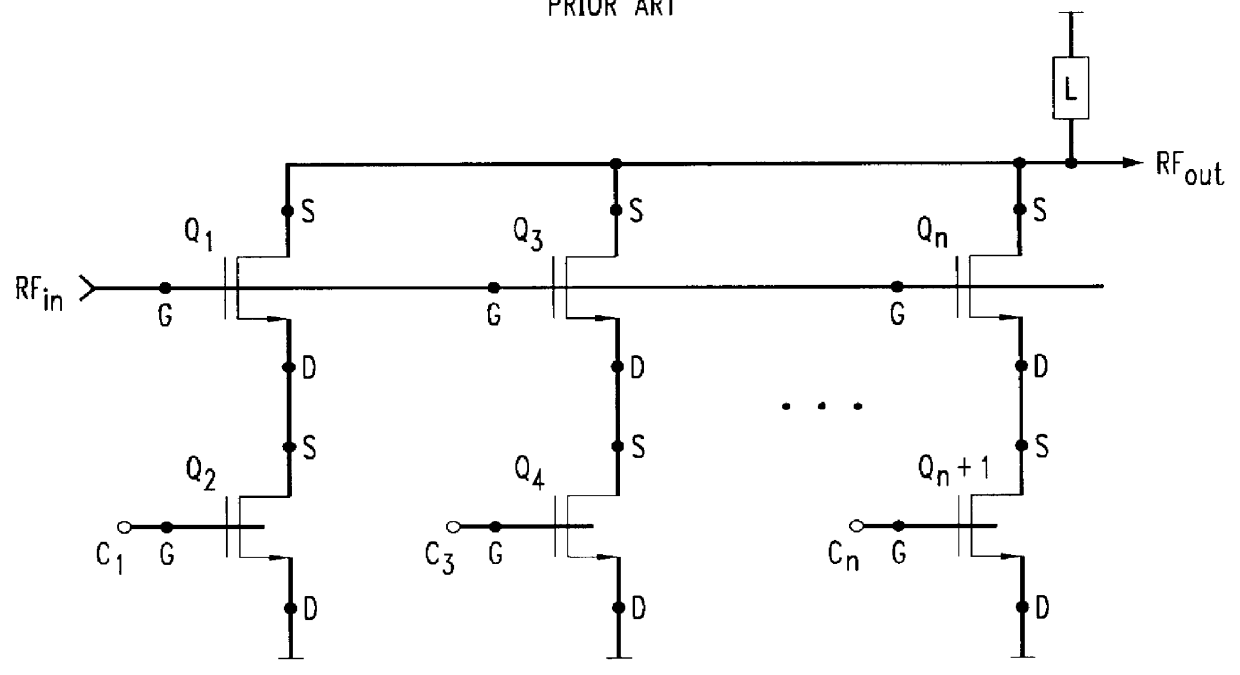
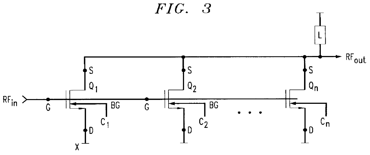
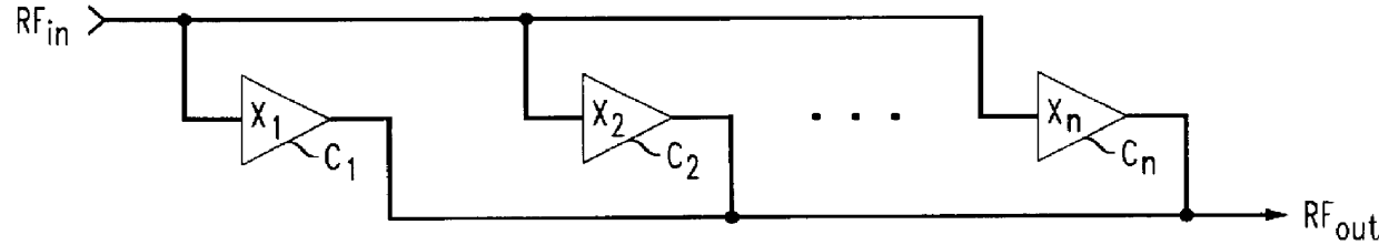
A schematic representation of a switched power amplifier circuit in accordance with a preferred embodiment of the present invention is shown in FIG. 3. The circuit includes a plurality of non-linear amplifier stages and, in particular, MOSFET transistors Q.sub.1 -Q.sub.n connected between a load "L" and a common terminal "x", e.g. ground. Each transistor Q has four terminals, namely, a source (S), a gate (G), a drain (D) and a backgate (BG).
It is known that each MOSFET transistor has an inherent impedance value. It is also known that by fixing the back-gate terminal (BG) at a potential--such as by tying it to the source terminal (S)--the transistor Q operates in a conventional manner, that is, the output or drain current from the drain terminal (D) is controlled by the voltage applied to the gate terminal (G). In addition, it is widely recognized that the threshold voltage of a MOSFET transistor is a fixed value when the backgate terminal is tied to a fixed voltage but that the thre...
PUM
 Abstract
Description
Claims
Application Information