Thin film resistor and fabrication method thereof

a thin film resistor and film technology, applied in the direction of resistors, semiconductor devices, electrical equipment, etc., can solve the problems of limited resistances that can be achieved, similar resistances, and limited resistance values of resistors,

Inactive Publication Date: 2000-05-30
GLOBALFOUNDRIES INC
View PDF24 Cites 61 Cited by
  • Summary
  • Abstract
  • Description
  • Claims
  • Application Information

AI Technical Summary

Problems solved by technology

Unfortunately, since the dopants and dosages applied to form resistors are limited by the device doping parameters, the resistances that can be achieved are similarly limited.
In addition, resistors are typically space-intensive so that the formation of resistors and the resistance values of the resistors are limited by the surface area of the substrate.

Method used


Image

  • Thin film resistor and fabrication method thereof
  • Thin film resistor and fabrication method thereof
  • Thin film resistor and fabrication method thereof

Examples


Embodiment Construction

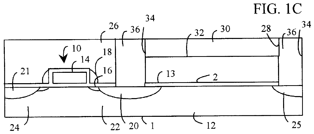
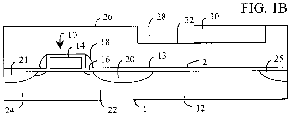
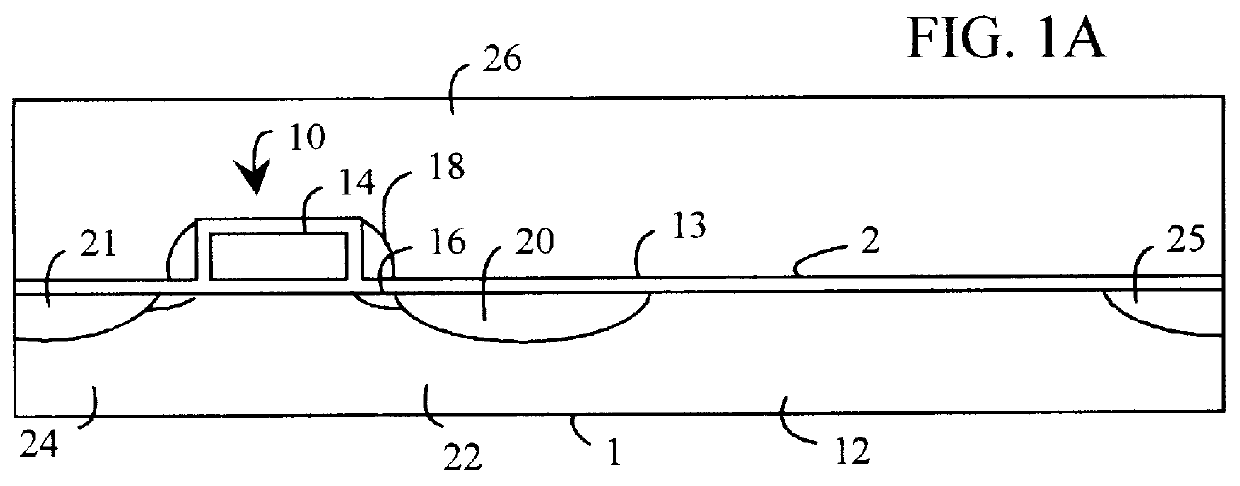
FIG. 1A depicts a portion of a semiconductor wafer 1 showing a cross-sectional view of a MOSFET 10 formed on a transistor layer 2 of a substrate 12. In an illustrative embodiment, the MOSFET 10 is formed using lightly-doped drain (LDD) fabrication techniques including formation of a gate oxide layer 13 overlying the substrate 12, formation of a polysilicon gate 14, and implant of LDD regions 16 in the substrate 12 self-aligned with the polysilicon gate 14. Silicon nitride or silicon dioxide spacers 18 are formed lateral to the polysilicon gate 14.

Following formation of the spacers 18, a heavily-doped drain implant 20 is implanted on a drain side 22 of the MOSFET 10. A source side 24 of the MOSFET 10 may be implanted with a heavily-doped source implant 21. An intralayer dielectric (ILD) layer of silicon dioxide 26 is deposited over the substrate 12 and the polysilicon gate 14 and spacers 18 to electrically isolate devices formed on the substrate 12. The ILD layer of silicon dioxide 2...


PUM


Abstract

A resistor is formed between devices in an integrated circuit by forming a patterned trench in an intralayer dielectric (ILD) deposited over the devices, filling the trench with polysilicon and planarizing the polysilicon. The resistance of the resistor is defined by determining and selecting the size and form of the trench including the width, length, depth and orientation of the trench. In some embodiments, the resistance of the resistor is also controlled by adding selected amounts and species of dopants to the polysilicon. In some embodiments, the resistance is controlled by directly saliciding the polysilicon in the trench.

Description

1. Field of the InventionThe present invention relates to an integrated circuit and fabrication method. More specifically, the present invention relates to an integrated circuit including a thin film resistor constructed in a plane elevated with respect to a device plane.2. Description of the Related ArtTypically resistors in integrated circuits are formed through a sequence including oxidation, masking, and doping steps in which a pattern is opened in a layer of oxide on a substrate surface. Resistors are often formed in the shape of dumbbells with square ends serving as contact regions with a long, thin region within which supplies resistance. The resistance of the interior long, thin region is determined from the sheet resistance of the region and the number of squares contained in the region. The number of squares is determined by dividing the length of the region by the width.Following doping and reoxidation, contact holes are etched in the square ends to contact the resistor i...

Claims


Application Information

Patent Timeline
Patent Type & Authority Patents(United States)
IPC IPC(8): H01L21/02H01L27/06
CPCH01L28/20H01L27/0688
Inventor KADOSH, DANIELGARDNER, MARK I.HAUSE, FREDERICK N.
Owner GLOBALFOUNDRIES INC
Why Eureka
Try Eureka