
Method for manufacturing compound semiconductor field-effect transistors with improved DC and high frequency performance

a technology of compound semiconductors and field-effect transistors, which is applied in the direction of semiconductor devices, basic electric elements, electrical equipment, etc., can solve the problems of robbing the device of its high-frequency efficiency, reducing the high-frequency performance, and neither the dc nor the high-frequency performance are optimized under this condition

Inactive Publication Date: 2000-07-04
THE UNITED STATES AS REPRESENTED BY THE DEPARTMENT OF ENERGY
View PDF1 Cites 14 Cited by
  • Summary
  • Abstract
  • Description
  • Claims
  • Application Information

AI Technical Summary

Problems solved by technology

This problem becomes more severe as the gate length of the transistor is reduced since carrier confinement is more difficult to realize, thus requiring an increased dose for the buried p-implant that in turn will degrade the high-frequency performance.
For conventional p-type implants (Be or Mg), however, neither the DC nor the high-frequency performance is optimized under this condition.
A drawback associated with this practice, however, concerns the fact that many of those atoms come to rest beyond the tail of the Si-channel and become active acceptors increasing C.sub.gs, and robbing the device of its high-frequency efficiency.
It is also known that carbon has a low activation efficiency.
Furthermore, the prior art does not incorporate this principle in semiconductor device structures to enhance performance.

Method used


Image

  • Method for manufacturing compound semiconductor field-effect transistors with improved DC and high frequency performance
  • Method for manufacturing compound semiconductor field-effect transistors with improved DC and high frequency performance
  • Method for manufacturing compound semiconductor field-effect transistors with improved DC and high frequency performance

Examples


Embodiment Construction

Carbon (.sup.12 C or .sup.13 C) is unique among p-type dopants in GaAs in that it occupies an As-site to become an electrically active acceptor. All other p-type-only impurities (excluding the amphoteric dopants Ge, Si and Sn) in GaAs (Be, Mg, Zn and Cd) occupy a Ga-site to become active acceptors. Unlike other p-type species that typically have close to 100% activation in GaAs, C, implanted by itself, in GaAs has a low activation efficiency of typically 50% or less (S. J. Pearton and C. R. Abernathy, Appl. Phys. Lett. 55, pp. 678-680, 1989).

This is for two reasons: First, since C is a relatively low mass ion it generates fewer vacancies during implantation compared to heavier ions. Second, As-vacancies have a higher energy of formation than Ga-vacancies (R. W. Jansen and O. F. Sankey, Phys. Rev. B, Vol. 39, pp. 3192-3206, 1989) and, therefore, fewer As-vacancies will be available for the C-ion to occupy, resulting in a reduction in C's activation efficiency as an acceptor.

The activ...


PUM


Abstract

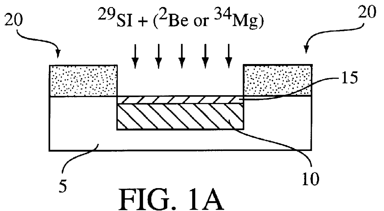
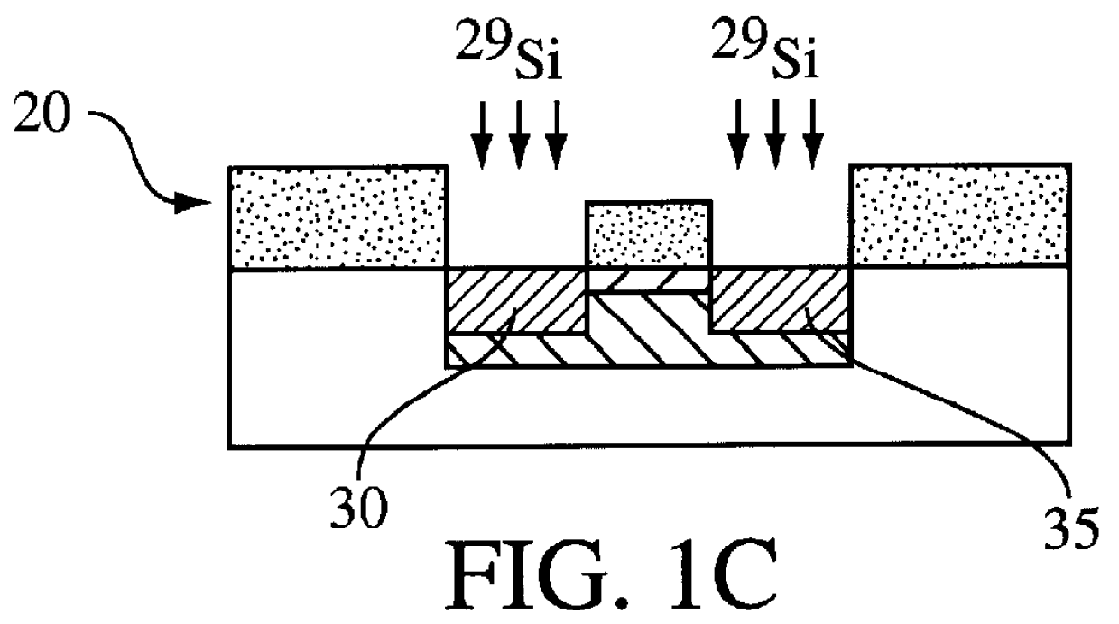
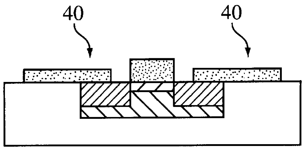
A method for making compound semiconductor devices including the use of a p-type dopant is disclosed wherein the dopant is co-implanted with an n-type donor species at the time the n-channel is formed and a single anneal at moderate temperature is then performed. Also disclosed are devices manufactured using the method. In the preferred embodiment n-MESFETs and other similar field effect transistor devices are manufactured using C ions co-implanted with Si atoms in GaAs to form an n-channel. C exhibits a unique characteristic in the context of the invention in that it exhibits a low activation efficiency (typically, 50% or less) as a p-type dopant, and consequently, it acts to sharpen the Si n-channel by compensating Si donors in the region of the Si-channel tail, but does not contribute substantially to the acceptor concentration in the buried p region. As a result, the invention provides for improved field effect semiconductor and related devices with enhancement of both DC and high-frequency performance.

Description

1. FIELD OF INVENTIONThis invention pertains to improving performance of compound semiconductor devices, generally, and more particularly to enhancing both DC and AC performance of field-effect transistor devices. Also provided is a method for efficiently producing these enhanced performance devices at lower cost than existing methods. In the preferred embodiment, carbon (C-ion) implants in gallium arsenide (GaAs) -based transistors are utilized both to sharpen the profile of a silicon (Si-ion) n-type channel and to minimize parasitic capacitances associated with buried p-regions. Use of the invention allows for improved DC and AC (high frequency) functioning of metal semiconductor field effect transistors (MESFETs), junction field effect transistors (JFETs) and other similar devices. Further, use of the methods described in fabricating the preferred embodiments will permit more efficient and less costly fabrication than currently used in competing methods while using the same manuf...

Claims


Application Information

Patent Timeline
IPC IPC(8): H01L21/265H01L21/02H01L21/338
CPCH01L21/26546H01L29/66863
Inventor ZOLPER, JOHN C.SHERWIN, MARC E.BACA, ALBERT G.
Owner THE UNITED STATES AS REPRESENTED BY THE DEPARTMENT OF ENERGY
Learn More