Electronic device and semiconductor package

a technology of electronic devices and semiconductors, applied in the field of electronic devices and semiconductor packages, can solve the problems of affecting the performance of semiconductor devices, bumps are fatigued, and breakage,

Inactive Publication Date: 2000-08-01
KK TOSHIBA
View PDF4 Cites 32 Cited by
  • Summary
  • Abstract
  • Description
  • Claims
  • Application Information

AI Technical Summary

Problems solved by technology

However, in an electronic device with a semiconductor package, a stress due to a thermal load that is applied in fabrication process or in operation concentrates at the solder balls 5 that connect the external connecting terminals of the semiconductor package and the connecting pads of the mother board and thereby the semiconductor package warps.
Thereby, the bumps are fatigued and broken.

Method used


Image

  • Electronic device and semiconductor package
  • Electronic device and semiconductor package
  • Electronic device and semiconductor package

Examples


embodiment 1

(Embodiment 1)

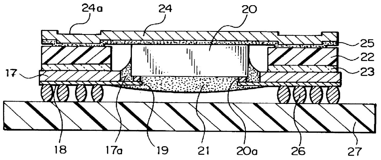
FIG. 1 is a sectional view showing the structure of principal portions of an electronic device according to a first embodiment of the present invention. In this embodiment, a tape-BGA type semiconductor package is mounted on a mother board.

In FIG. 1, reference numeral 17 is an insulating resin film. The insulating resin film 17 is composed of a polyimide resin film or the like. The insulating resin film 17 has a device hole 17a. Wirings 18 (for signal lines) and inner leads 19 are disposed on one main face (the lower face in FIG. 1). One edge portion of the inner leads 19 protrudes to the device hole 17a.

The other (rear) edge portion of the inner leads 19 is connected to the respective wirings 18. Connecting pads (not shown) as external connecting terminals are disposed at the other end of the wirings 18. A number of connecting pads are arranged in a grid pattern. A semiconductor element 20 is disposed with face down in the device hole 17a of the wiring film. Electrode...

embodiment 2

(Embodiment 2)

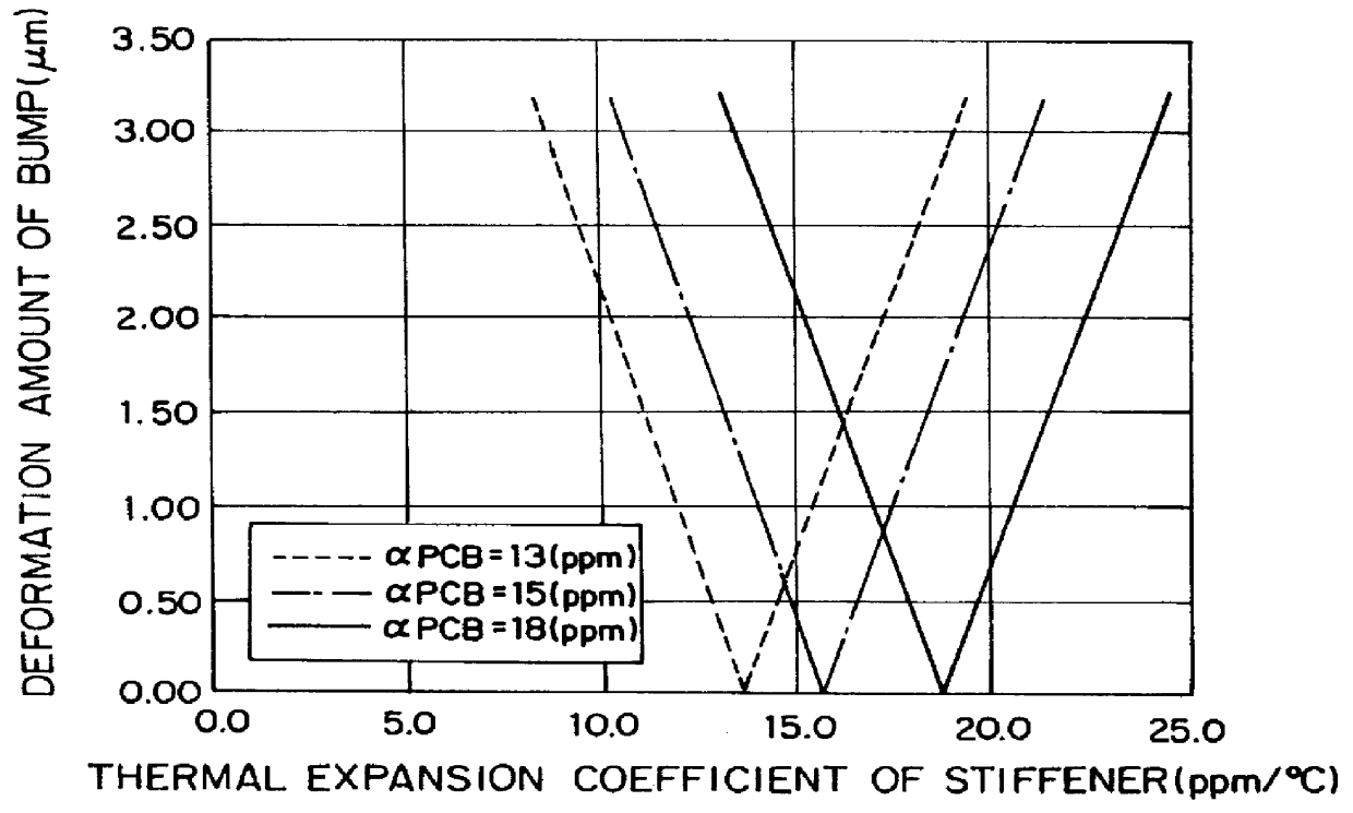
FIG. 3 shows principal portions of a semiconductor package according to a second embodiment of the present invention. In FIG. 3, similar parts to those in FIG. 1 are denoted by similar reference numerals. A heat radiating cap (stiffener unified heat radiating cap) 28 that has a shape-holding characteristic is disposed on a semiconductor element 20 and an insulating film 17. The heat radiating cap 28 is adhered to the upper face of the semiconductor element 20 and the insulating film 17 with an adhesive agent layer 23 composed of for example polyester. The stiffener unified heat radiating cap 28 is composed of a metal having TEC of 13.times.10.sup.-6 to 17.times.10.sup.-6 / K. Examples of the material of the heat radiating cap 28 is SUS 310S and CDA Alloy C15150.

In this embodiment, the semiconductor package is mounted on a glass-epoxy wiring substrate 27, and predetermined terminals are connected with solder bumps 26. Thus, they can be connected with high reliability. In...


PUM

PropertyMeasurementUnit
thicknessaaaaaaaaaa
temperature cycle testsaaaaaaaaaa
thicknessaaaaaaaaaa

Abstract

The electronic device has a structure that a semiconductor package is mounted on a mother board. To relieve stress caused by cyclic thermal load and applied to solder bumps that are electrically and mechanically connect the semiconductor package and the mother board, a shape-holding plate (stiffener) adhered to a wiring film is composed of a metal with a thermal expansion coefficient of 13x10-6 to 17x10-6 almost close to that of a glass-epoxy wiring substrate as the mother board. Examples of the metal are 25Cr-20Ni stainless steel or copper alloy containing 0.01 to 0.03% by weight of Zr.

Description

1. Field of the InventionThe present invention relates to an electronic device, in particular, to an electronic device of which a semiconductor package is mounted on a wiring substrate as a mother board with high reliability. In addition, the present invention relates to a semiconductor package, in particular, to a semiconductor package that is mounted on a wiring substrate as a mother board with high reliability.2. Description of the Related ArtTo decrease the size of an electronic device and compact circuit structure thereof, a semiconductor element (for example, an IC chip) is mounted on a multi-layered wiring substrate composed of ceramics or the like. The mounted area is sealed with a metal cap or molding resin.Particularly, in a semiconductor element such as a CPU that consumes a high power, a heat sink is disposed so as to give off heat from the element.In addition, to reduce the cost of the fabrication of an electronic device and simplify the structure thereof, a TCP (tape c...

Claims


Application Information

Patent Timeline
Patent Type & Authority Patents(United States)
IPC IPC(8): H01L23/10H01L23/495H01L23/34H01L23/31H01L23/02H01L23/28H01L23/373H01L23/48H05K1/18H01L21/60H01L23/12
CPCH01L23/10H01L23/3128H01L23/3171H01L23/3736H01L23/49572H01L23/49582H01L2224/16H01L2224/48091H01L2224/48247H01L2224/73253H01L2924/01079H01L2924/15153H01L2924/1517H01L2924/15311H01L2924/1532H01L2924/00014H01L24/48H01L2924/01019H01L2224/45099H01L2924/181H01L2924/00012H01L2224/0401H01L23/00
Inventor IKEMIZU, MORIHIKOOIE, NOBUAKIIWASAKI, KEN
Owner KK TOSHIBA
Why Eureka
Try Eureka