Transistor with integrated poly/metal gate electrode

a technology of metal and polysilicon gate electrodes, applied in the field of semiconductor processing, can solve the problems of affecting the packing density and parasitic overlap capacitance between the gate and source/drain region, polysilicon has the disadvantage of a much higher resistivity than aluminum, and the rc time constant and dc voltage variation are undetectable in vlsi or ulsi circuits

Inactive Publication Date: 2000-09-12
ADVANCED MICRO DEVICES INC
View PDF8 Cites 21 Cited by
  • Summary
  • Abstract
  • Description
  • Claims
  • Application Information

AI Technical Summary

Problems solved by technology

The switch to polysilicon as a gate electrode material was the result of certain disadvantages associated with aluminum in early fabrication technologies.
This alignment procedure can adversely affect both packing density and parasitic overlap capacitances between the gate and source / drain regions.
Despite the several advantages of polysilicon over aluminum as a gate electrode material, polysilicon has the disadvantage of a much higher resistivity as compared to aluminum.
Higher resistivity translates into higher values of interconnect line resistance that can lead to undesirably long RC time constants and DC voltage variations within VLSI or ULSI circuits.
However, the resistivity of polysilicon gate electrodes in conventional MOS integrated circuit processing still presents a potential impediment to successful process scaling through reductions in the operating voltages of VLSI and ULSI devices.
Another disadvantage of polysilicon as a gate electrode material is polysilicon depletion.
If the amount of boron diffused is sufficiently high, the electrical performance of the MOSFET may be severely degraded due to polysilicon depletion.

Method used


Image

  • Transistor with integrated poly/metal gate electrode
  • Transistor with integrated poly/metal gate electrode
  • Transistor with integrated poly/metal gate electrode

Examples


Embodiment Construction

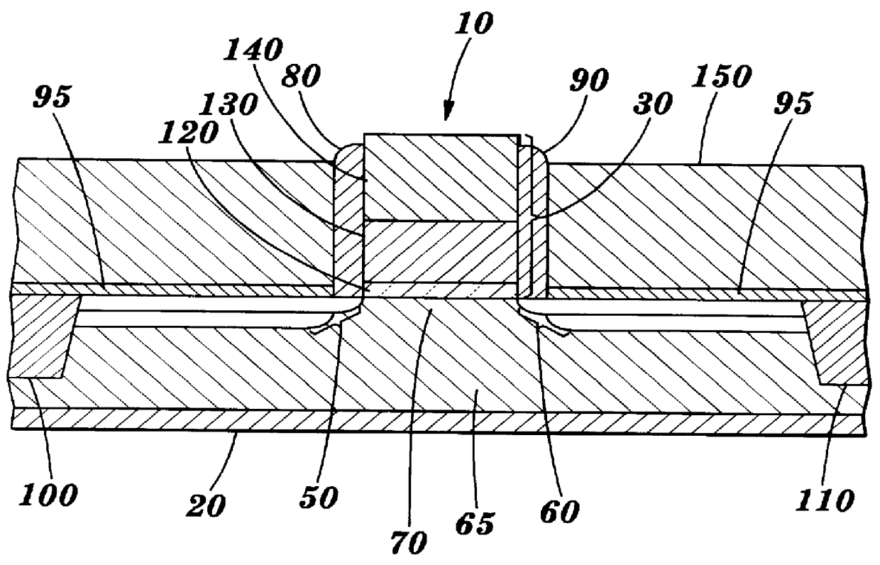
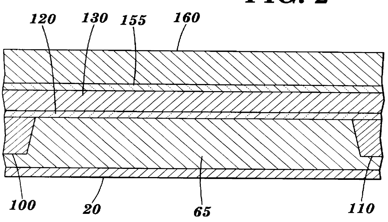
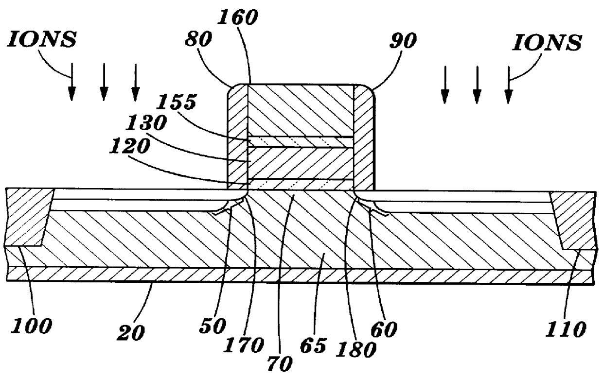
In the drawings described below, reference numerals are generally repeated where identical elements appear in more than one figure. Turning now to the drawings, and initially to FIG. 1, there is shown a cross-sectional view of an exemplary embodiment of an integrated circuit transistor ("transistor") 10 in accordance with the present invention. The transistor 10 may be an IGFET, a MOSFET, or other type of transistor and may be n-channel or p-channel. The transistor 10 is formed on a semiconductor substrate 20 which may be composed of n-doped, or p-doped silicon, silicon-on-insulator, or other suitable substrate materials. The transistor 10 includes a gate electrode stack 30 formed on the substrate 20. First and second source / drain regions 50 and 60 are formed in a well 65 in the substrate 20 and are laterally spaced to define a channel region 70 underlying the gate electrode stack 30. The well 65 may be a N-well or a P-well. Insulating sidewall spacers 80 and 90 are disposed adjacen...


PUM


Abstract

An integrated circuit transistor and method of making the same are provided. The transistor includes a substrate, first and second source/drain regions, and a gate electrode stack coupled to the substrate. The gate electrode stack is fabricated by forming a first insulating layer on the substrate, forming a first conductor layer on the first insulating layer, and forming a metal layer on the first conductor layer. A second insulating layer, such as an interlevel dielectric layer, is coupled to the substrate adjacent to the gate electrode stack. Sidewall spacers and LDD processing may be incorporated. The transistor and method integrate metal and polysilicon into a self-aligned gate electrode stack.

Description

1. Field of the InventionThis invention relates generally to semiconductor processing, and more particularly, to a method of fabricating an integrated circuit transistor with an integrated metal and polysilicon gate electrode stack.2. Description of the Related ArtInsulated gate field effect transistors ("IGFET"), such as metal oxide semiconductor field effect transistors ("MOSFET"), are some of the most commonly used electronic components in modern integrated circuits. Embedded controllers, microprocessors, analog-to-digital converters, and many other types of devices now routinely include millions of MOSFETs. The dramatic proliferation of MOSFETs in integrated circuit design can be traced to their high switching speeds, potentially low power dissipation, and adaptability to semiconductor process scaling.A typical MOSFET implemented in silicon consists of a source and a drain formed in a silicon substrate, and separated laterally to define a channel region in the substrate. A gate ...

Claims


Application Information

Patent Timeline
Patent Type & Authority Patents(United States)
IPC IPC(8): H01L21/28H01L21/02H01L21/336
CPCH01L21/28061H01L29/665H01L29/66545H01L29/66575H01L29/6659
Inventor GARDNER, MARK I.WRISTERS, DERICK J.CHEEK, JON D.
Owner ADVANCED MICRO DEVICES INC
Why Eureka
Try Eureka