Driving method for optical apparatus

Inactive Publication Date: 2000-10-17
CANON KK
View PDF13 Cites 31 Cited by
  • Summary
  • Abstract
  • Description
  • Claims
  • Application Information

AI Technical Summary

Problems solved by technology

The brightness modulation scheme is not readily applicable to a device using an optical modulation substance having a steep transmittance change characteristic or a memory characteristic.
Further, the brightness modulation using a TN-liquid crystal is not suitable for a system dealing with data varying at high speeds because the TN-liquid crystal generally has a low response speed.
The pixel division scheme equivalent to a system using a unit pixel comprising an assemblage of pixels, is caused to

Method used


Image

  • Driving method for optical apparatus
  • Driving method for optical apparatus
  • Driving method for optical apparatus

Examples


reference example 1

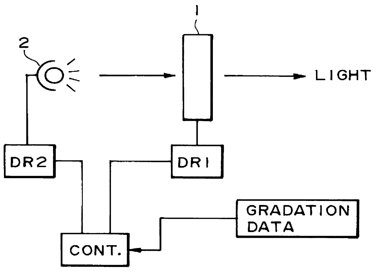
FIG. 10 illustrates an optical modulation system for driving an optical modulation device. The system includes a liquid crystal device 101 comprising a pair of substrate each having thereon an electrode and a chiral smectic liquid crystal disposed between the substrates, and a gradation data-generating circuit 103 for generating gradation data, and a light source 105. In front of the system, an observer 105 is indicated. The system also includes a drive circuit including a capacitive element C.sub.PC and a transistor 102, whose source-drain (or emitter-collector) resistance is changed by changing the gate or base potential of the transistor 102, thereby changing a time point at which the voltage exceeds the inversion threshold of the liquid crystal. The drive circuit includes a voltage application means V.sub.ext for applying a reset voltage and drive voltages to the liquid crystal device. C.sub.flc represents a capacitance of the liquid crystal.

The gradation data-generating circuit...

reference example 2

FIG. 12 illustrates another embodiment of optical modulation system. The system includes a reflection-type liquid crystal device 201 comprising a pair of substrates each having thereon an electrode and a liquid crystal disposed between the substrates, a light source-drive circuit 204 for driving a light source, a capacitive element C.sub.PC, a resistive element R.sub.PC, and a drive voltage supply Vd. In this system, a circuit is constituted so that the resistive element R.sub.PC is caused to have varing resistance value, which varies depending on inputted gradation data.

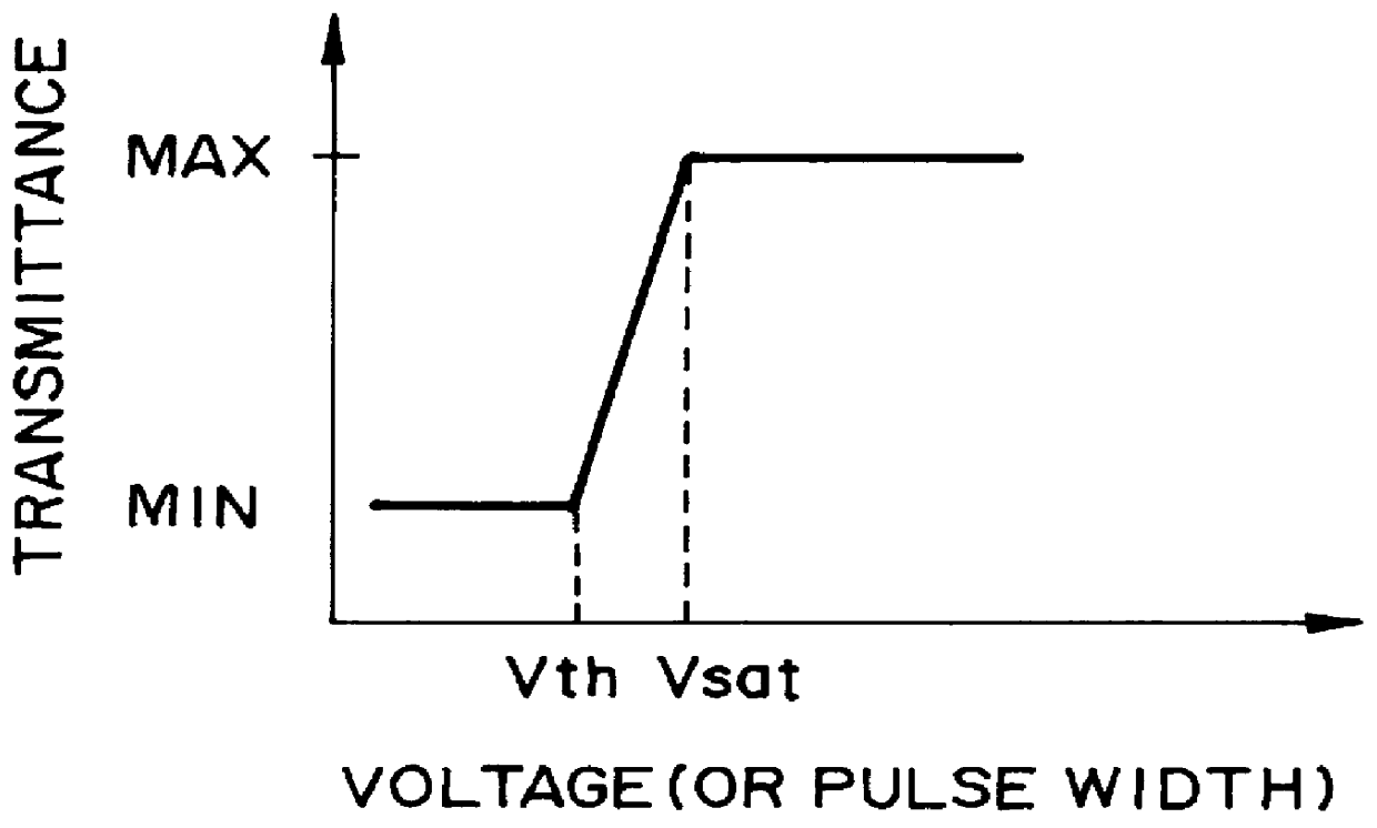
The liquid crystal used may have a transmittance-applied voltage (T-V) characteristic, as shown in FIG. 9A.

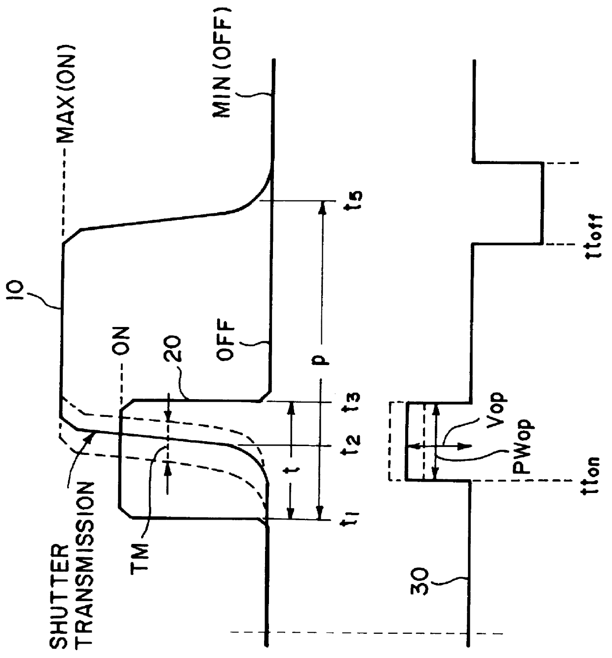
FIG. 13 is a time chart for driving the system of FIG. 12. V.sub.S1 represents the application time of voltage Vd, V.sub.lc represents a voltage applied to the liquid crystal, T.sub.ran represents a reflectance of the liquid crystal device, 204T represents a lighting time of the light source, and 205T represent...

reference example 3

FIG. 14 illustrates another example of optical modulation system. The system includes a reflection-type liquid crystal device 301 comprising a pair of substrates each having thereon an electrode and a liquid crystal disposed between the substrates, a light source-drive circuit 304 for driving a light source, a capacitive element C.sub.PC, a resistive element R.sub.PC, a drive voltage supply Vv and a switch V.sub.SO for turning on and off the supply of a voltage signal from the drive voltage supply Vv . In this system, the voltage signal supplied from the drive voltage supply Vv carries analog gradation data.

The liquid crystal used may have a transmittance-applied voltage (T-V) characteristic as shown in FIG. 9A.

FIG. 15 is a time chart for driving the system of FIG. 14. V.sub.SO represents an application time of gradation signal, V.sub.lc represents a voltage applied to the liquid crystal, T.sub.ran represents a reflectance of the liquid crystal device, 304T represents a lighting tim...


PUM


Abstract

An optical apparatus includes an optical modulation means having a pair of electrodes, and a photoconductor layer and an optical modulation substance layer disposed between the electrodes, a signal light source for supplying light data carrying gradation data to the photoconductor layer, and a readout light illuminator for supplying readout light for reading out picture data to the optical modulation substance layer. The readout light illuminator is driven so as to supply readout light having a planar light intensity distribution providing a constant product of a gradation period and a readout light intensity at each readout site of the optical modulation substance, or so as to scan the photoconductor layer with the light data frame by frame in mutually different scanning directions in succeeding frames.

Description

FIELD OF THE INVENTION AND RELATED ARTSThe present invention relates to a driving method for an optical apparatus, and particularly to a driving method for an optical apparatus including an optical modulation means for modulating optical states based on signals including gradation data, and a readout light source for supplying readout light for reading picture data to the optical modulation means.An optical modulation device (optical modulation means) is included in various optical apparatus, such as a display apparatus. Gradational display or gray-scale display is performed by using such an optical modulation device, for example according to various schemes as will be described hereinbelow with reference to a liquid crystal display device as a familiar example.Accordingly to one scheme, a twisted nematic (TN) liquid crystal is used as an optical modulation element (substance) constituting pixels and voltage data is applied to the TN-liquid crystal to modulate (control) the transmit...

Claims


Application Information

Patent Timeline
IPC IPC(8): G02F1/13G02F1/135G09G3/36G09G3/34H04N9/31H04N5/74G09G3/20
CPCG02F1/135H04N9/3197G09G3/3406G09G3/36H04N5/7416H04N9/3155G09G3/02G09G3/2007G09G3/2014G09G3/2081G09G3/34G09G3/3614G09G2300/0473G09G2310/0235G09G2310/0237G09G2310/061G09G2360/142
Inventor YAGYU, MINETO
Owner CANON KK
Why Eureka
Try Eureka