Asymmetric transfer molding method and an asymmetric encapsulation made therefrom

a transfer molding and asymmetric technology, applied in the field of encapsulation methods of articles, can solve the problems of sensitive electronic devices and limited symmetrical design of mold configurations

Inactive Publication Date: 2000-11-07
MICRON TECH INC
View PDF5 Cites 44 Cited by
  • Summary
  • Abstract
  • Description
  • Claims
  • Application Information

AI Technical Summary

Problems solved by technology

It is well known that electronic devices are sensitive and thus require protection from physical and environmental conditions which may degrade or completely ruin them.
Howe...

Method used


Image

  • Asymmetric transfer molding method and an asymmetric encapsulation made therefrom
  • Asymmetric transfer molding method and an asymmetric encapsulation made therefrom
  • Asymmetric transfer molding method and an asymmetric encapsulation made therefrom

Examples


Embodiment Construction

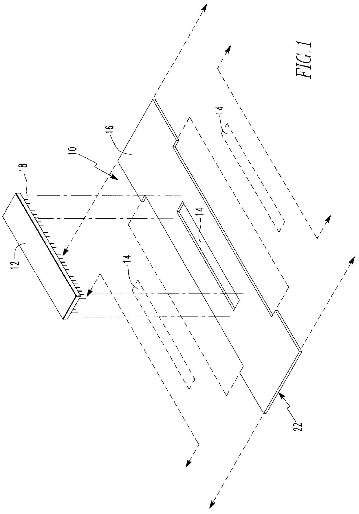
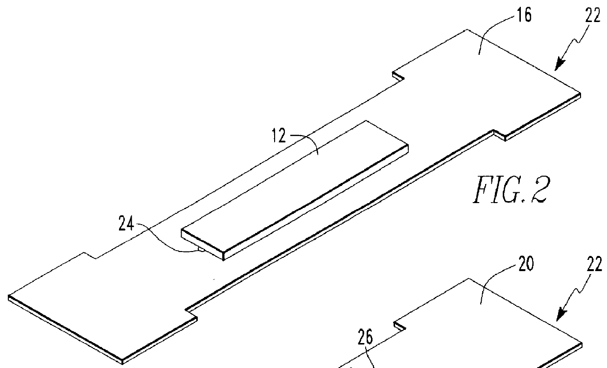
FIG. 1 illustrates a substrate 10 which may be used in conjunction with the method of the present invention. The description of the method of the present invention in connection with the substrate 10 is for purposes of illustration only, and not limitation. It is anticipated that the method and molds of the present invention may be used to encapsulate a large variety of articles, both electrical and non-electrical. In FIG. 1, the substrate is a known flexible substrate suitable for receiving electrical devices 12 in openings 14. The electrical device may be any type of device, although a memory device is shown in FIG. 1.

The electrical device 12 may be connected to a first side 16 of the substrate 10 by any known means, e.g. lamination, adhesion, etc. The device 12 may be of a type in which electrical connections extend from the center of the device. The device 12 is positioned such that the electrical connections 18 of the device 12 extend through opening 14 to a second side 20 of s...


PUM

PropertyMeasurementUnit
Flexibilityaaaaaaaaaa
Moldableaaaaaaaaaa
Surface areaaaaaaaaaaa

Abstract

A method of encapsulating an article having first and second surfaces, includes positioning a first molding section in a sealing relationship with the first surface of the article and positioning a second molding section adjacent the second surface of the article. The first molding section is filled first thereby forcing the second surface of the article into a sealing engagement with the second molding section. The second molding section is then filled.

Description

1. Field of the InventionThe invention relates to a method of encapsulating an article and, more specifically, to transfer molding an asymmetric encapsulation for an electronic device, and an asymmetric encapsulated electronic device.2. Description of the BackgroundIt is well known that electronic devices are sensitive and thus require protection from physical and environmental conditions which may degrade or completely ruin them. Therefore, it is well known in the art to protect electronic devices from these conditions by sealing them with a protective encapsulation material. This "packaging" of the electronic devices protects them from the conditions which may degrade them and allows the devices to be transported and handled, and thus allows them to be easily configured with other components. Several encapsulation methods are known in the art such as under-fill encapsulation (for flip chip applications) and glob topping.One prior-art method for encapsulating devices is the "transf...

Claims


Application Information

Patent Timeline
IPC IPC(8): H01L21/56H01L23/31H01L21/00H01L21/02H01L23/29H01L23/28
CPCH01L21/56H01L23/293H01L23/3121B29C45/14418B29C45/14655H01L21/565Y10T428/23H01L2224/4824H01L2924/14H01L2924/1433H01L2924/15311H01L24/48B29C2045/14672Y10T428/239Y10T428/1352H01L2924/181H01L2224/05599H01L2224/85399H01L2924/00014H01L2924/00012H01L2224/45099H01L2224/45015H01L2924/207
Inventor JOHNSON, MARK S.BOLKEN, TODD O.
Owner MICRON TECH INC
Why Eureka
Try Eureka