Method for addressing electrical fuses

a technology for electrical fuses and circuits, applied in static storage, digital storage, instruments, etc., can solve the problems of increasing the relative cost of the memory system within the computer, the inability to repair further defects occurring subsequently up to and including the final packaging of the chip, and the inability to fully function. the effect of the chip is simple and efficien

Inactive Publication Date: 2000-12-26
IBM CORP +1
View PDF3 Cites 35 Cited by
  • Summary
  • Abstract
  • Description
  • Claims
  • Application Information

AI Technical Summary

Benefits of technology

It is a further objective of the invention to provide a simple and efficient method of providing a high voltage adequate for blowing th...

Problems solved by technology

Today multi-media requires at least a 64 MB, and preferably even a 128 MB memory, which increases the relative cost of the memory system within the computer.
As DRAM density and lithographic difficulties increase, it is more difficult to have a fully...

Method used


Image

  • Method for addressing electrical fuses
  • Method for addressing electrical fuses
  • Method for addressing electrical fuses

Examples


Embodiment Construction

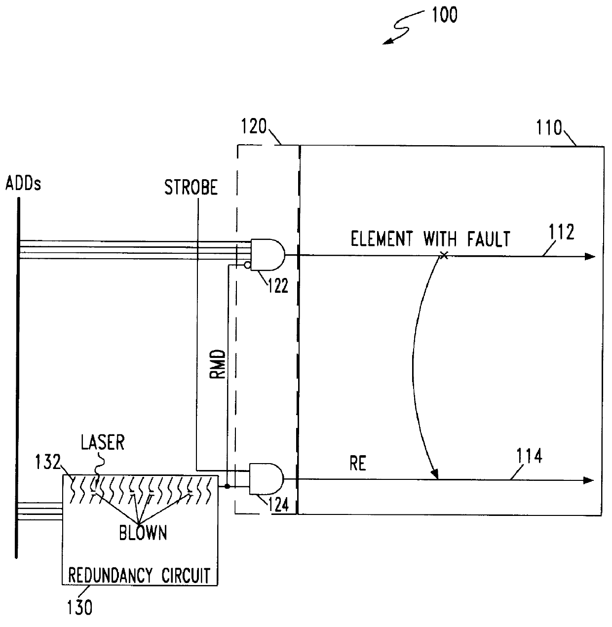
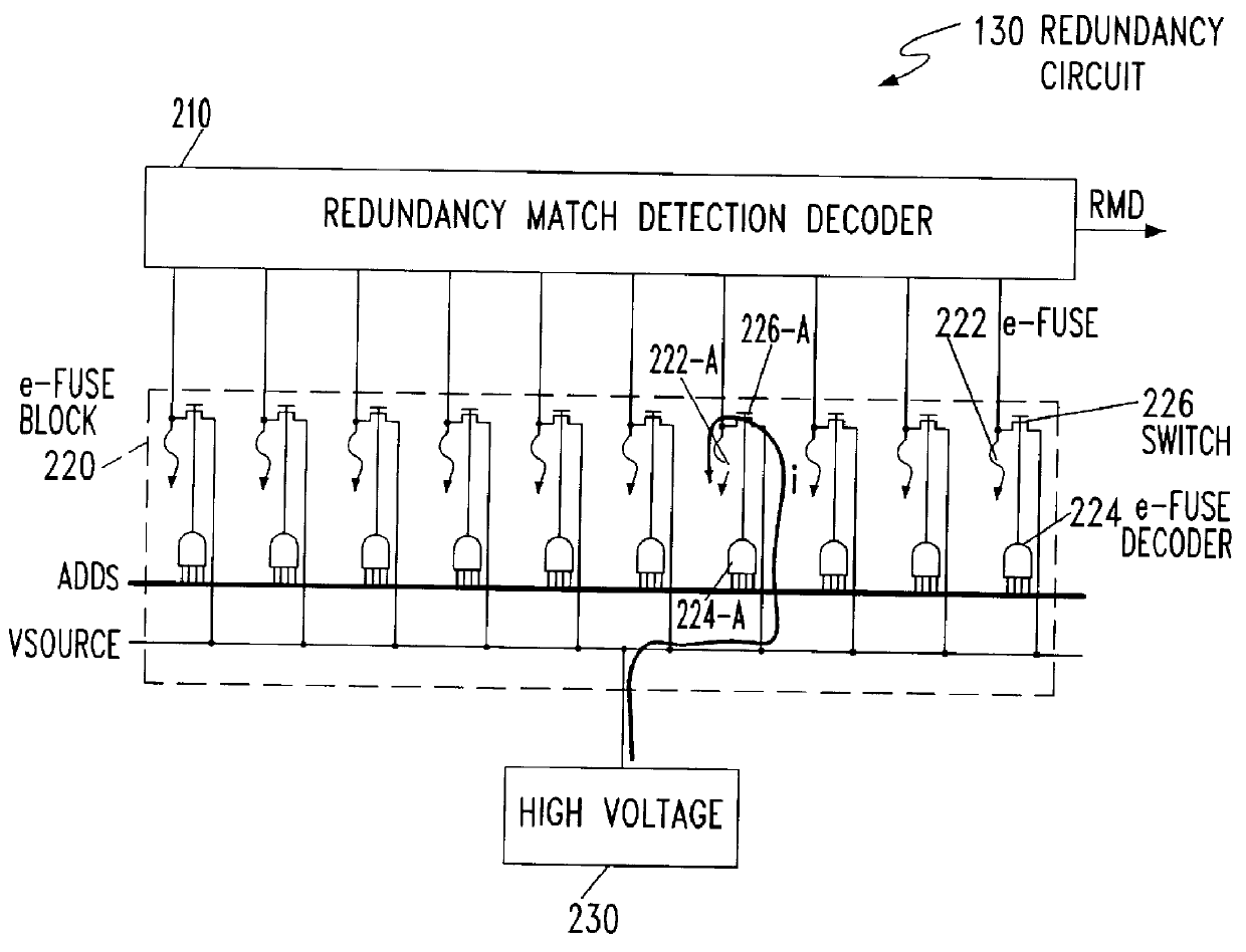
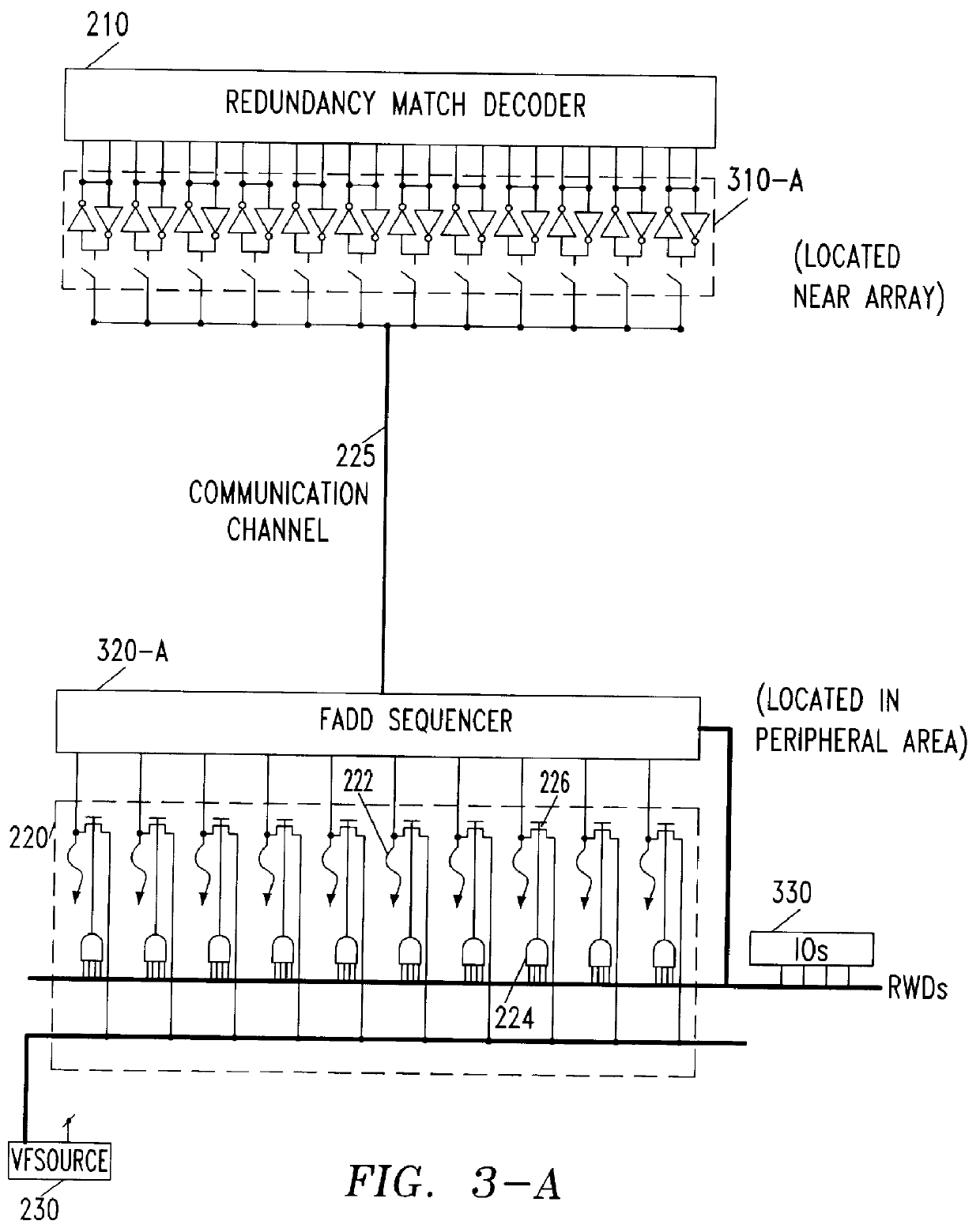
FIG. 3A shows a first preferred embodiment of the invention. Unlike existing e-fuse architectures, a redundancy match detection decoder (210) coupled to an e-fuse block (220) are placed near the array, preferably, at the periphery of the chip. The redundancy match detection decoder (210) and the e-fuse bank (220) are coupled to a communication channel (225). More particularly, the e-fuse bank (220) consists of a plurality of e-fuses (222). Unlike the conventional approach, the input of the e-fuse decoders (224) use a plurality of Read / Write Data bus (RWDs 235). Thus, the selection of e-fuses to be blown is determined by the RWDs buses which are coupled to corresponding input and output ports (I / Os). The I / O terminals and RWDs are common to the memory cell read / write operation, as it is known in a conventional memory. More particularly, while in memory write mode, the data from the I / O ports is transferred to the corresponding RWDs, allowing the data to be written to the memory arr...


PUM


Abstract

A memory device that includes a plurality of data storage cells; at least one redundancy data storage cell; a redundancy match detection circuit; and a means for coupling programmable fuses to the redundancy match detection circuit, wherein a defective data storage is replaced by one redundancy data storage when the redundancy match detection detects a pre-determined condition set by said programmable fuse is described. Decoding is accomplished by a data bus selecting the e-fuse to be blown. The data bus is also used for reading the state of the e-fuses to ensure that the e-fuses are correctly blown. Power is effectively applied to the selected e-fuses while sharing the data bus for e-fuse decoding and verification. In order to reduce the number of communication channels between e-fuses and the redundancy match detection circuitry, the transfer operation uses time multiplexing, allowing e-fuse information to be transferred to the redundancy match detection circuitry sequentially. The actual time multiplexing operation for performing the transfer is preferably enabled only after the chip power-up state.

Description

This invention generally relates to a redundancy replacement architecture for memory devices, and more particularly, to an electrically programable redundancy replacement configuration applicable to large scale memories.CMOS technology has evolved such that the computer market has rapidly opened to a wide range of consumers. Today multi-media requires at least a 64 MB, and preferably even a 128 MB memory, which increases the relative cost of the memory system within the computer. In the near future, it is likely that 256 MB and 512 MB computers will become commonplace, which suggests a potential strong demand for 256 Mb DRAMs (Dynamic Random Access Memory) and beyond. Still in the development stage, DRAMs in the Gigabit range are already under way. As DRAM density and lithographic difficulties increase, it is more difficult to have a fully functional DRAMs. This necessitates the introduction of new techniques that guarantee a reasonable chip yield notwithstanding the added complexit...

Claims


Application Information

Patent Timeline
IPC IPC(8): G11C29/00G11C11/413G11C11/401G11C29/04
CPCG11C29/802G11C29/00
Inventor KIRIHATA, TOSHIAKIDANIEL, GABRIEL
Owner IBM CORP
Why Eureka
Try Eureka