Method of manufacturing a sensor detecting a physical action as an applied force

a manufacturing method and sensor technology, applied in the direction of force measurement using piezo-resistive materials, instruments, force measurement, etc., can solve the problems of affecting the reliability of measured values, affecting the output characteristic with respect to respective axial directions, and affecting the accuracy of measurement results

Inactive Publication Date: 2001-02-13
OKADA KAZUHIRO
View PDF44 Cites 79 Cited by
  • Summary
  • Abstract
  • Description
  • Claims
  • Application Information

AI Technical Summary

Benefits of technology

In accordance with the above described signal processing circuit, a characteristic matrix showing the condition of interference produced between components in respective axial directions and an inverse characteristic matrix of the inverse matrix thereof are determined in advance. Further, corrective operations using this inverse characteristic matrix are carried out, thereby making it possible to cancel the influence of interference. Furthermore, since these corrective operations are all carried out at the analog computation circuit, the circuit configuration becomes simple and a correction circuit can be realized at a low cost. In addition, because operation is performed in an analog form, the operation speed becomes high, giving rise to no inconvenience even in the case of measuring an instantaneous phenomenon.
In accordance with the sixth feature, a plurality of unit areas are defined on the first substrate, and the processing proceeds at the same time with respect to respective plurality of unit areas. Finally, one unit area will constitute one sensor unit. A plurality of grooves are dug in a longitudinal direction and in a lateral direction on the second plane surface of the first substrate, respectively. Within each unit area, respective four grooves are formed along four boundary sides of the working area or the fixed area. By these grooves, flexibility is given to the flexible area. Since it is sufficient to form grooves longitudinally and laterally in a matrix form, these grooves can be easily dug by mechanical processing. Thus, precise grooves can be efficiently formed.

Problems solved by technology

However, the conventional force sensors (or acceleration sensors, or magnetic sensors based on the same principle) have the problem that there may occur interference in the output characteristic with respect to respective axial directions of two-dimensions or three-dimensions.
In the case of conventional sensors, however, these components in respective axial directions interfere with each other.
Such an interference is not preferable because it lowers reliability of measured values.
However, the test for the acceleration sensor or the magnetic sensor becomes more complicated.
This results in the problem that the testing device becomes large, and a test for a dynamic acceleration of vibration is only conducted.
Further, conventionally proposed sensors using resistance elements has a problem in the case of carrying out high sensitivity measurement.
However, in the case of the structure of conventional sensors, it was difficult to enlarge the working body.
In the case of the high sensitivity sensor, where a large force more than a predetermined limit is applied thereto, the danger that the semiconductor substrate may be damaged is increased For this reason, it is necessary to provide, around the working body, a member for allowing displacement of the working body to limitatively fall within a predetermined range.
This gives another problem that the structure becomes complicated.

Method used


Image

  • Method of manufacturing a sensor detecting a physical action as an applied force
  • Method of manufacturing a sensor detecting a physical action as an applied force
  • Method of manufacturing a sensor detecting a physical action as an applied force

Examples


Embodiment Construction

.sctn.1 BASIC STRUCTURE OF THE SENSOR

1.1 Structure of the Acceleration Sensor

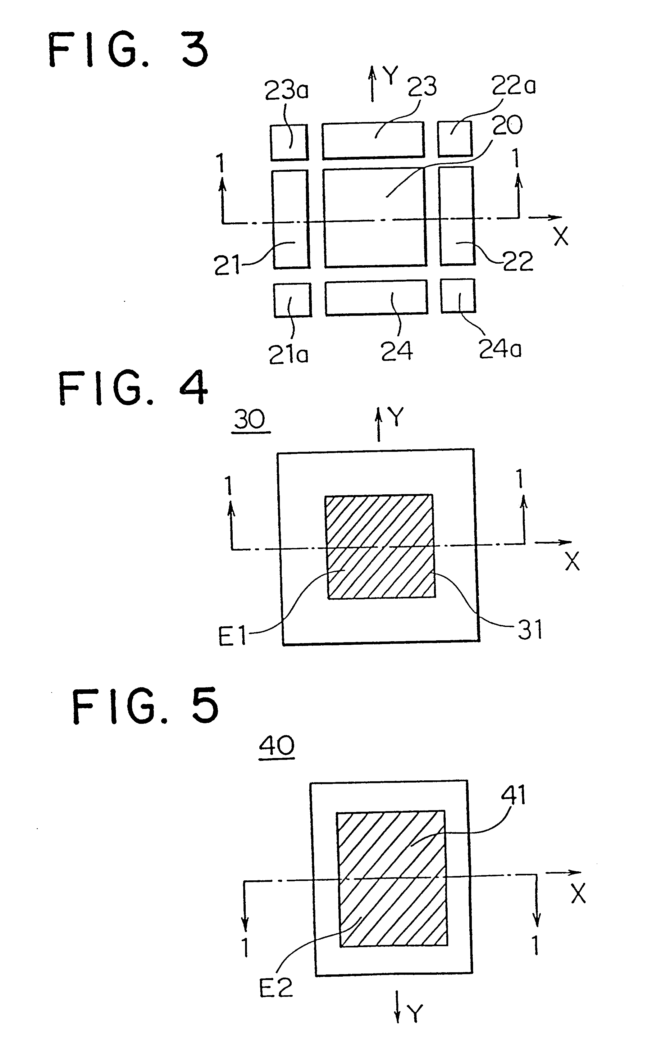
This invention can be widely applied, in general, to an apparatus for detecting a physical quantity exerted as an external force, and can be utilized not only to a force sensor but also to an acceleration sensor, or a magnetic sensor. In other words, all sensors are common in the basic structure of the central portion thereof. Accordingly, the object to which this invention is applied will be briefly described by taking an example of an acceleration sensor.

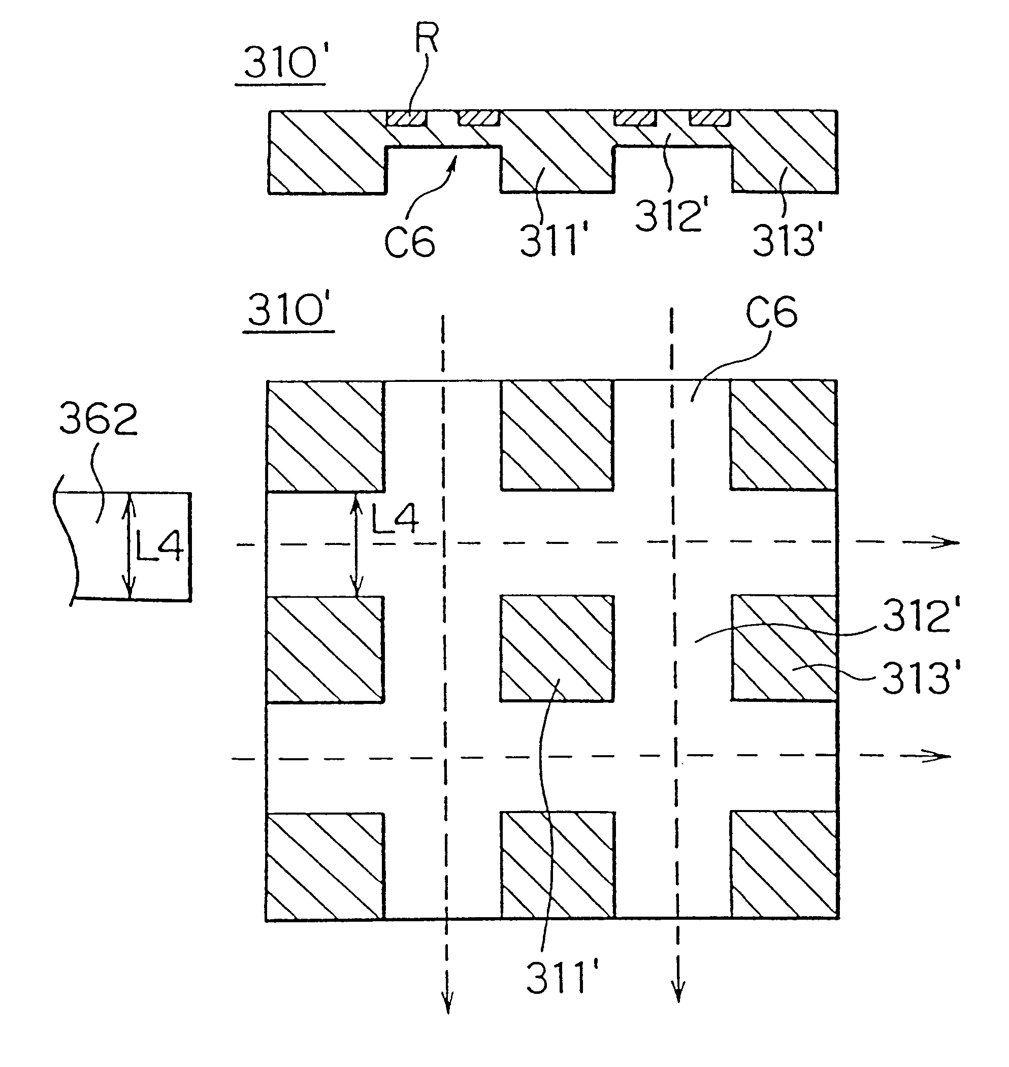
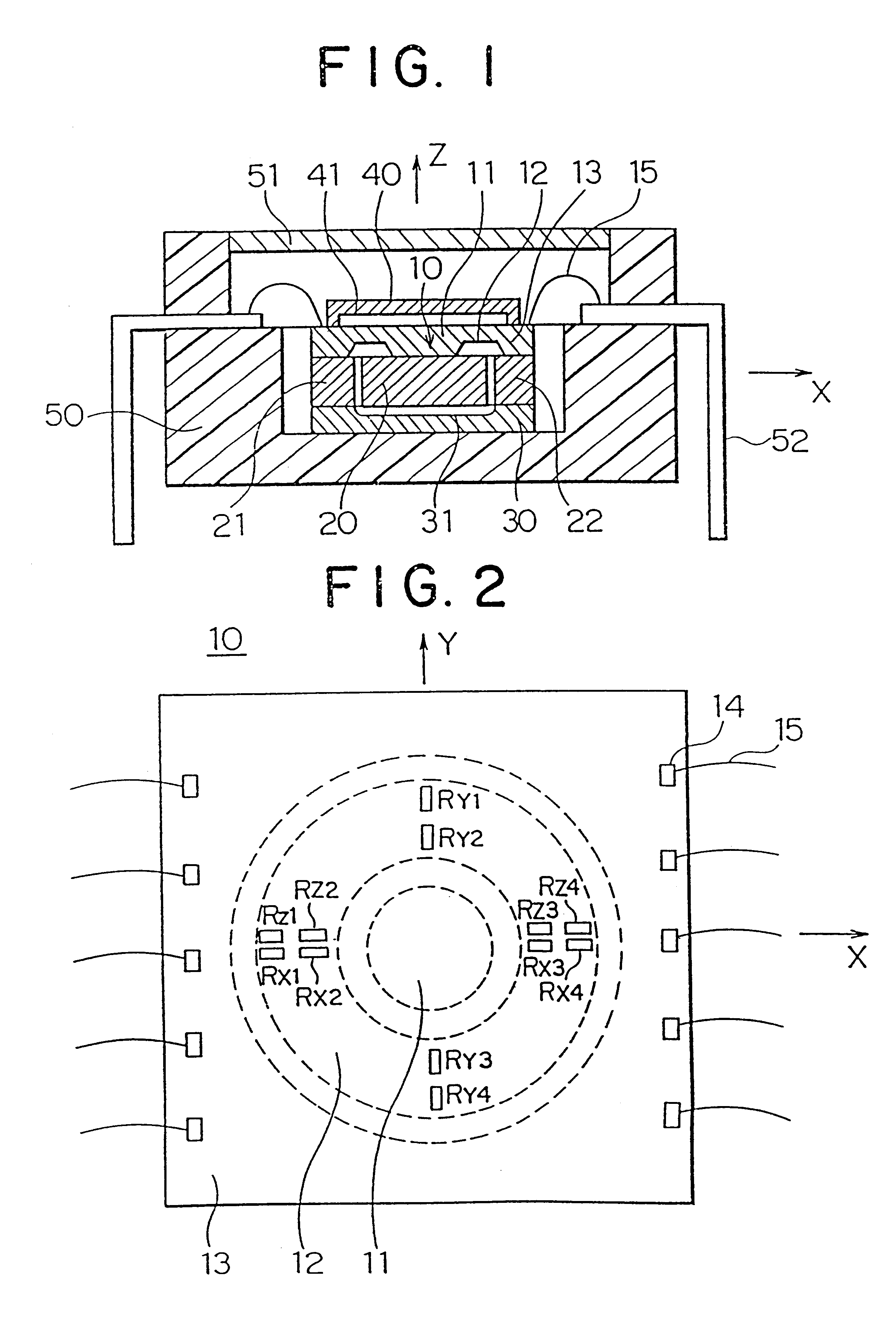
FIG. 1 is a structural cross sectional view showing an example of an acceleration sensor. The component serving as the central unit of this sensor is a semiconductor pellet 10. In this example, a single crystal substrate of silicon is used. The top view of the semiconductor pellet 10 is shown in FIG. 2. The cross section of the semiconductor pellet 10 shown at the central portion of FIG. 1 corresponds to the cross section cut along the X-axis of FIG. 2. T...


PUM

PropertyMeasurementUnit
angleaaaaaaaaaa
widthaaaaaaaaaa
mechanical deformationaaaaaaaaaa

Abstract

A sensor comprises a semiconductor pellet (10) including a working portion (11) adapted to undergo action of a force, a fixed portion (13) fixed on the sensor body, and a flexible portion (13) having flexibility formed therebetween, a working body (20) for transmitting an exterted force to the working portion, and detector means (60-63) for transforming a mechanical deformation produced in the semiconductor pellet to an electric signal to thereby detect a force exerted on the working body as an electric signal. A signal processing circuit is applied to the sensor. This circuit uses analog multipliers (101-109) and analog adders / subtracters (111-113), and has a function to cancel interference produced in different directions. Within the sensor, two portions (E3, E4-E8) located at positions opposite to each other and producing a displacement therebetween by action of a force are determined. By exerting a coulomb force between both the portions, the test of the sensor is carried out. Further, a pedestal (21, 22) is provided around the working body (20). The working body and the pedestal are located with a predetermined gap or spacing therebetween. A displacement of the working body is caused to limitatively fall within a predetermined range corresponding to the spacing. The working body and the pedestal are provided by cutting a same common substrate (350, 350')

Description

This invention relates to an apparatus for detecting a physical quantity acting as an external force, e.g., a force exerted on a working body, an acceleration exerted on a weight body, or a magnetism exerted on a magnetic body. Particularly, this invention relates to a signal processing circuit, a testing method, and a manufacturing method for a force sensor serving as a main part of such a detector, and a structure of this force sensor.In recent years, there are proposed force sensors including, arranged on a semiconductor substrate, resistance elements having a property of the piezo resistive effect that the electric resistance varies in dependency upon a mechanical deformation to detect a force from changes in resistance values of the resistance elements. Further, acceleration sensors or magnetic sensors to which such force sensors are applied are also proposed. In either detector, a strain generative body partially having flexibility is used to detect a mechanical deformation pr...

Claims


Application Information

Patent Timeline
Patent Type & Authority Patents(United States)
IPC IPC(8): G01L25/00G01L5/16G01P21/00G01P15/125G01P15/18G01P15/12G01L1/18G01L1/14
CPCG01L1/148G01L1/18G01L5/162G01L25/00G01P15/125G01P15/18G01P21/00G01P15/123Y10T29/49103G01P2015/084
Inventor OKADA, KAZUHIRO
Owner OKADA KAZUHIRO
Why Eureka
Try Eureka