

Small electrode for a chalcogenide switching device and method for fabricating same
- Summary
- Abstract
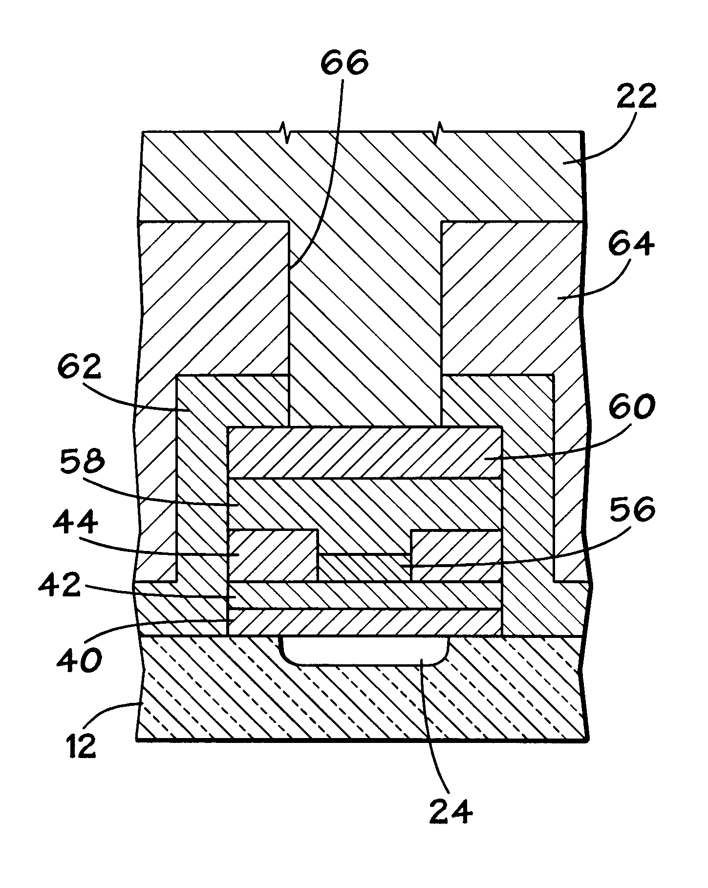
- Description
- Claims
- Application Information
AI Technical Summary
Problems solved by technology
Method used
Image

Examples
Embodiment Construction
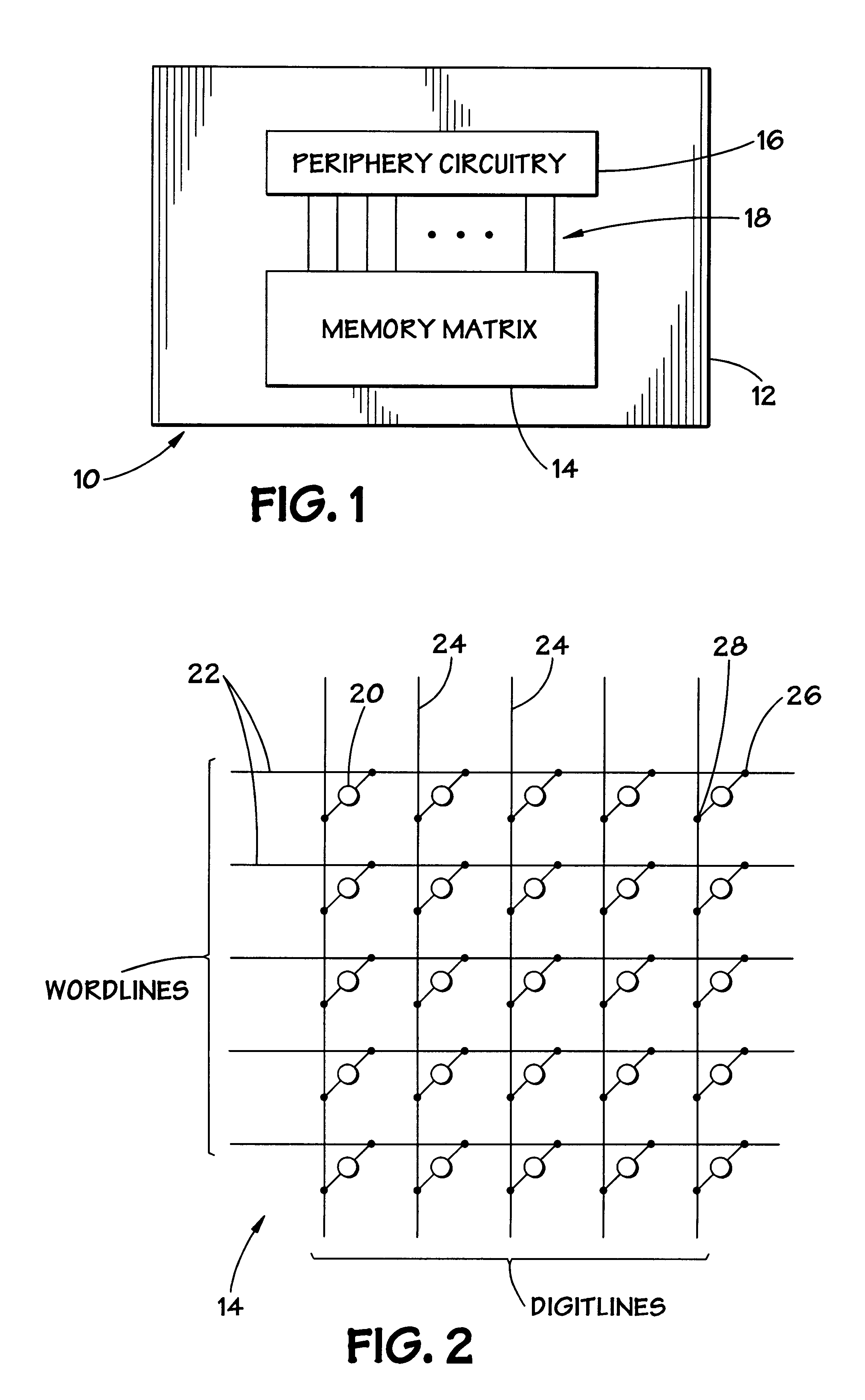
Turning now to the drawings, and referring initially to FIG. 1, a memory device is illustrated and generally designated by a reference numeral 10. The memory device 10 is an integrated circuit memory that is advantageously formed on a semiconductor substrate 12. The memory device 10 includes a memory matrix or array 14 that includes a plurality of memory cells for storing data, as described below. The memory matrix 14 is coupled to periphery circuitry 16 by the plurality of control lines 18. The periphery circuitry 16 may include circuitry for addressing the memory cells contained within the memory matrix 14, along with circuitry for storing data in and retrieving data from the memory cells. The periphery circuitry 16 may also include other circuitry used for controlling or otherwise insuring the proper functioning of the memory device 10.
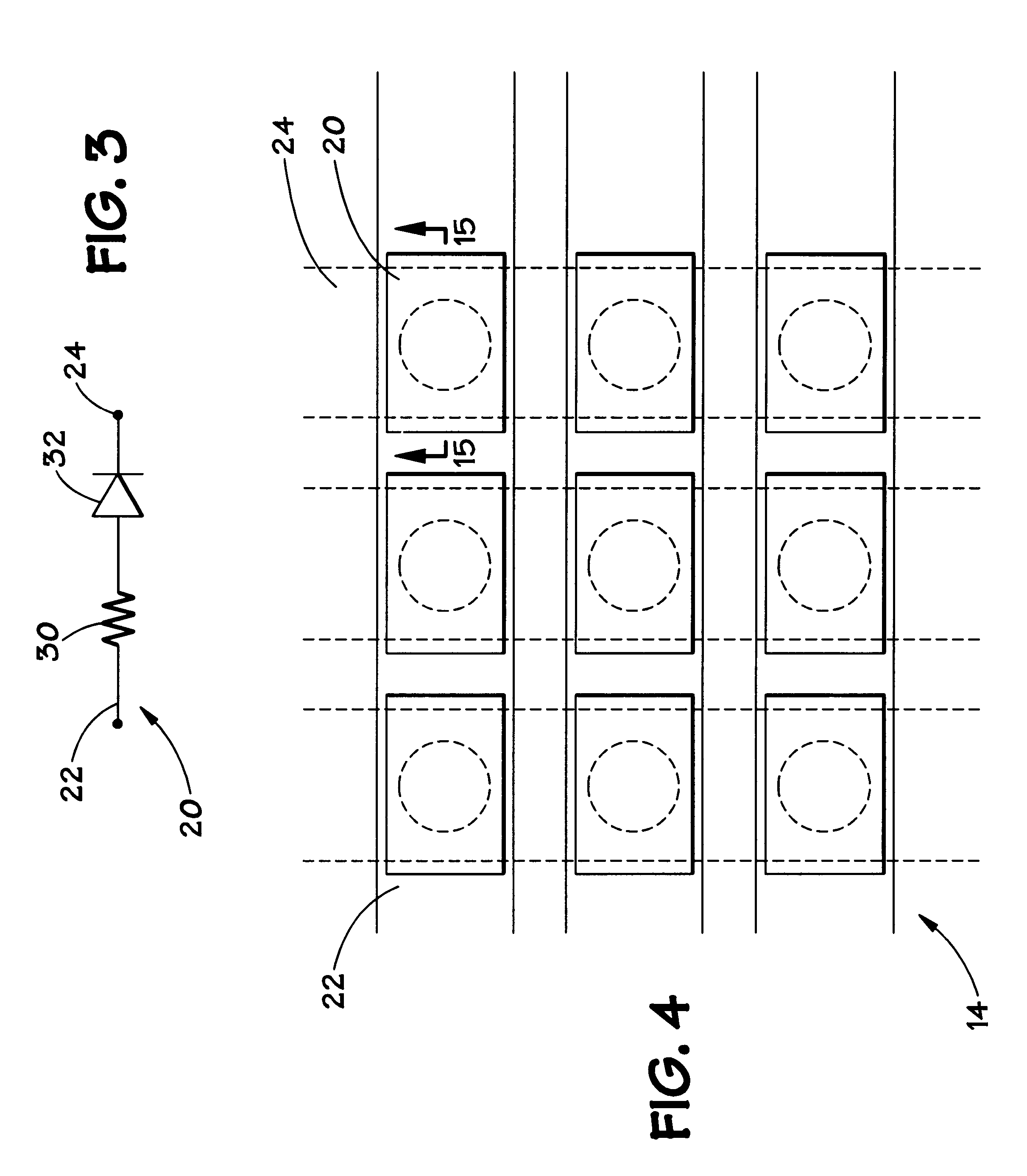
A more detailed depiction of the memory matrix 14 is illustrated in FIG. 2. As can be seen, the memory matrix 14 includes a plurality of memory ce...
PUM
 Abstract
Description
Claims
Application Information