

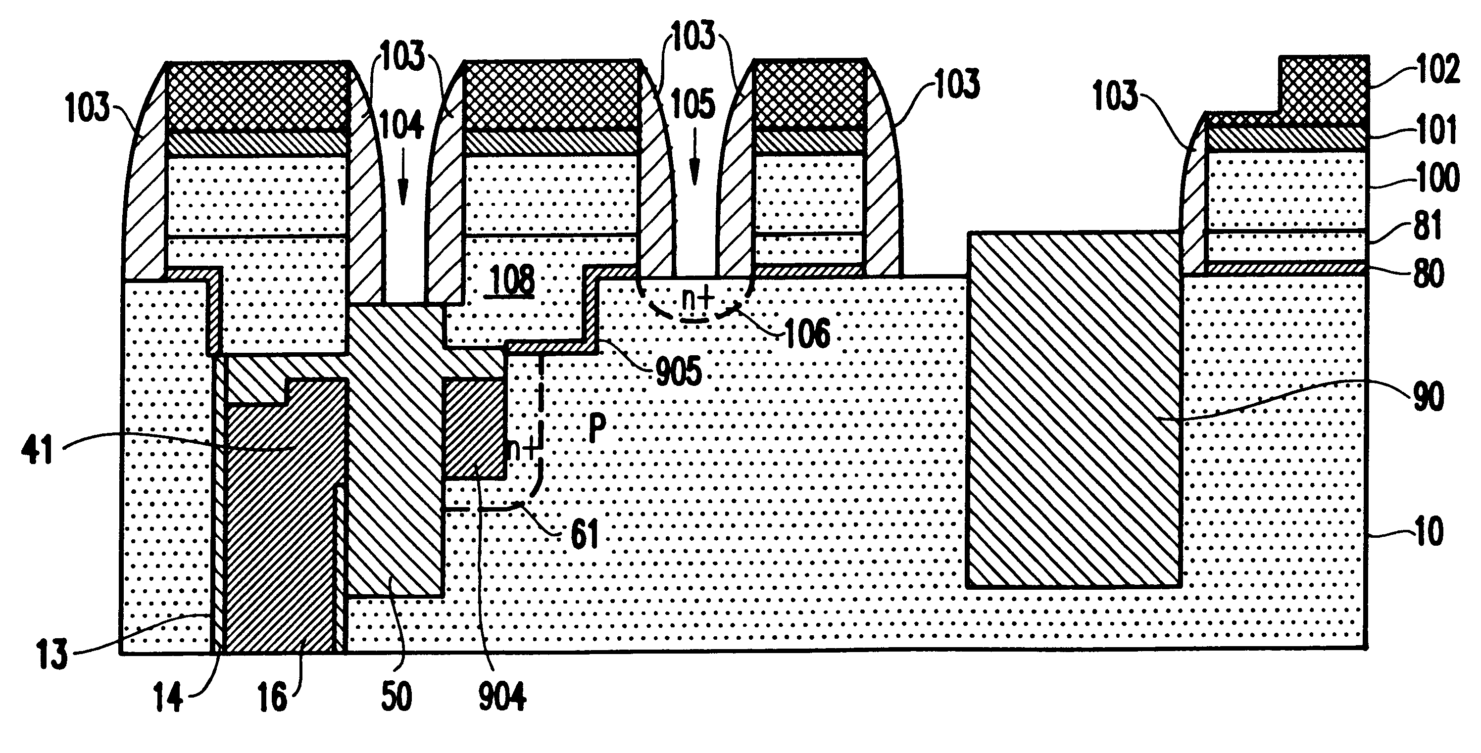
Formation of 5F2 cell with partially vertical transistor and gate conductor aligned buried strap with raised shallow trench isolation region
a technology of partially vertical transistors and gate conductors, applied in the field of integrated circuits, can solve the problems of strap formation and substantial problems of conventional vertical transistors
- Summary
- Abstract
- Description
- Claims
- Application Information
AI Technical Summary
Benefits of technology
Problems solved by technology
Method used
Image

Examples
Embodiment Construction
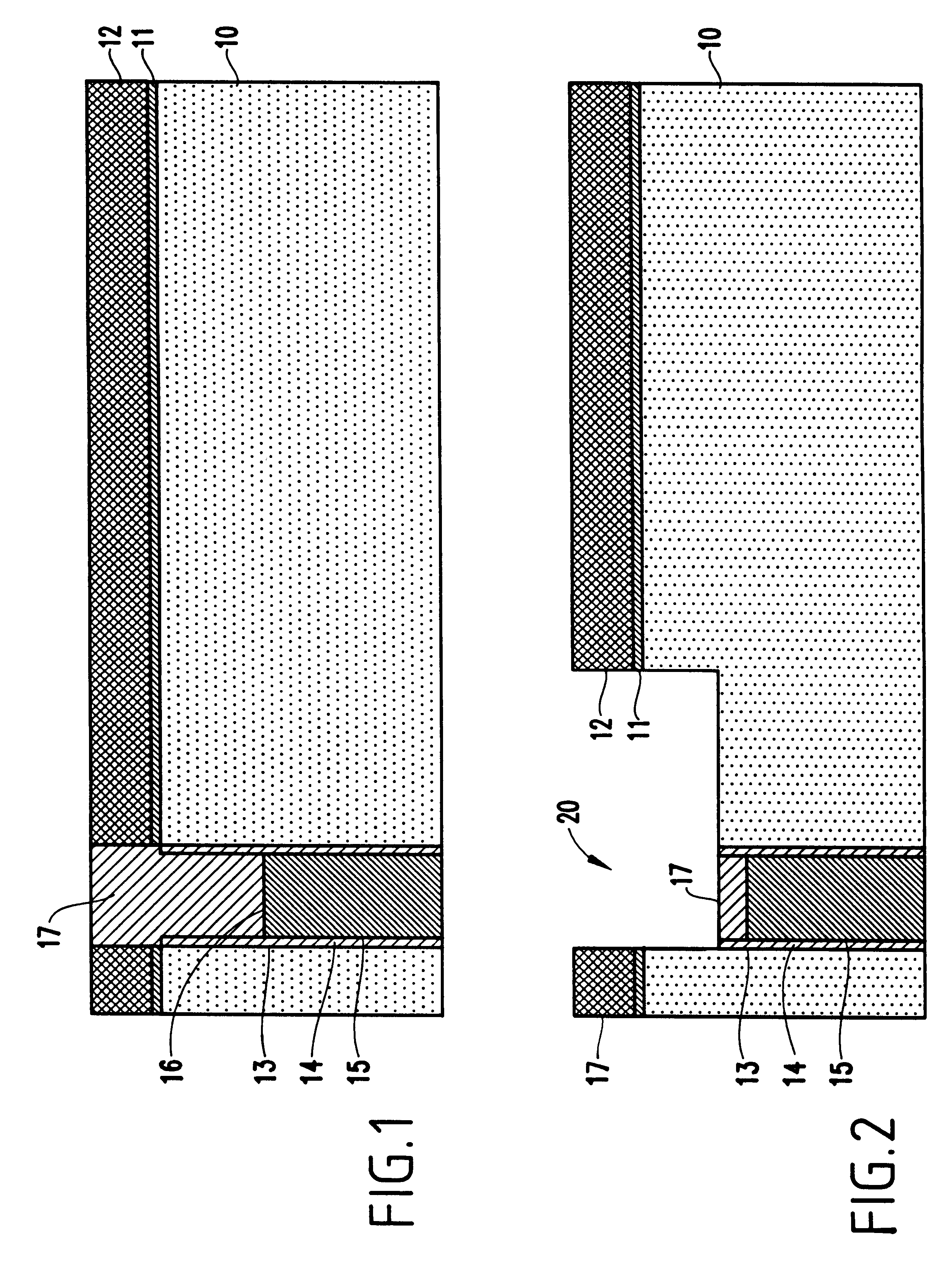
Referring now to the drawings, and more particularly to FIG. 1, a partially formed transistor according to a first embodiment of the invention is illustrated. More specifically, FIG. 1 illustrates a silicon substrate 10 upon which a first insulator 11 (such as a pad oxide) and a second insulator 12 (such as a pad silicon nitride) are formed.
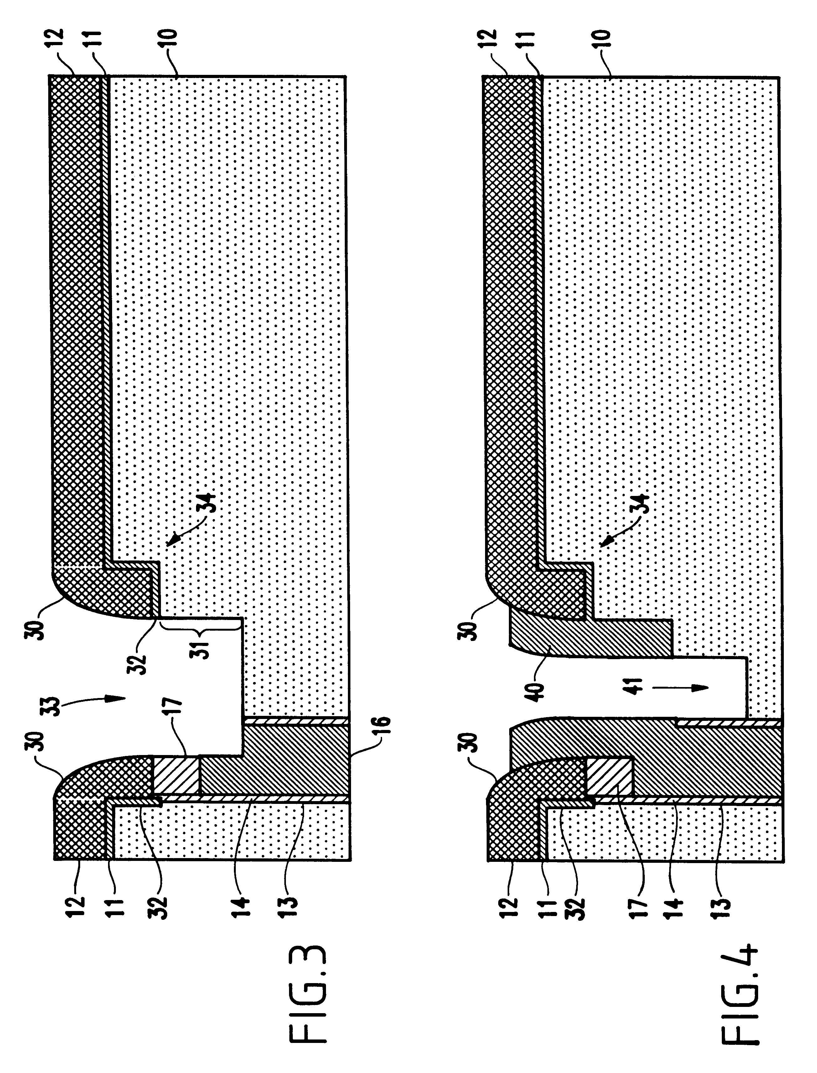
Using processes well known to those ordinarily skilled in the art, a trench 13 is formed in the substrate 10. Such conventional processes could include photolithographic masking and conventional etching techniques. The upper portion (e.g., top 1.5 .mu.m) of the trench, 13 is then lined with a thin (e.g., 30 nm thick) insulating collar 14 (such as a collar oxide). The insulating collar 14 is then recessed within the trench to a point just below the first insulator layer 11. A conductive material 16 (such as polysilicon, metal or alloy) is then deposited in the trench 13 and the structure is planarized using, for example, chemical mechanical polish...
PUM
 Abstract
Description
Claims
Application Information