Semiconductor device with field shield electrode

a technology of shield electrode and semiconductor, applied in the direction of semiconductor devices, electrical devices, transistors, etc., can solve the problems of device reliability, various reliability problems are left unsolved, and the device operating speed is affected

Inactive Publication Date: 2001-02-20
MITSUBISHI ELECTRIC CORP
View PDF19 Cites 16 Cited by
  • Summary
  • Abstract
  • Description
  • Claims
  • Application Information

AI Technical Summary

Benefits of technology

The first object of the present invention is to provide a semiconductor device with field-shield isolation structure which has no problem of deterioration in operation characteristics and reliability of the device due to existence of the FS insulating layer. The second object of the present invention is to provide a semiconductor device with field-shield isolation structure which is capable of preventing a breakage of the gate oxide film due to its manufacturing process. The third object of the present invention is to provide a semiconductor device which is capable of preventing a short circuit between the FS electrode and the gate electrode due to the material of the FS electrode. Another object of the present invention is to provide methods suitable for manufacturing these semiconductor devices.

Problems solved by technology

As a result, there arises a problem in terms of reliability of device, such as generation of leak current.
In the background-art field-shield isolation structure, various problems are left unsolved in terms of reliability due to its structure and its manufacturing method.
As the FS upper oxide film 41 becomes thinner, the parasitic capacitance between the FS electrode 5 and the gate electrode 6 increases, to cause degradation of operating speed of the device and increase likelihood of short circuits between these electrodes.
As the FS electrode 5 becomes thinner, its electrical resistance increases and there is a possibility of not achieving the desired performance during device operation with insufficient effect of field-shield isolation.
If the exfoliated silicide film 12 comes into conductive dust, and remains on the semiconductor device, the remainder ill affects the operation characteristics of the semiconductor device and deteriorates production yield of the device.
Moreover, if the FS electrode 5 is partially lost together with the exfoliated silicide film 12, that causes a break in the FS electrode 5 resulting in lower production yield of the device.
The oxide films OF3 and OF1, however, may be removed by dry etching at the same time, though this causes the following problem.
That results in less reliability of the gate oxide film and by extension, less reliability of the MOS transistor with field-shield isolation structure.
Besides the above problem, there is another problem, due to the material of the FS electrode, of a short circuit between electrodes which occurs at a portion where the gate electrode of the transistor overlaps the FS electrode.
That causes an operation failure of the MOS transistor and loses the function of a protective circuit.

Method used


Image

  • Semiconductor device with field shield electrode
  • Semiconductor device with field shield electrode
  • Semiconductor device with field shield electrode

Examples


Embodiment Construction

on SOI Device>

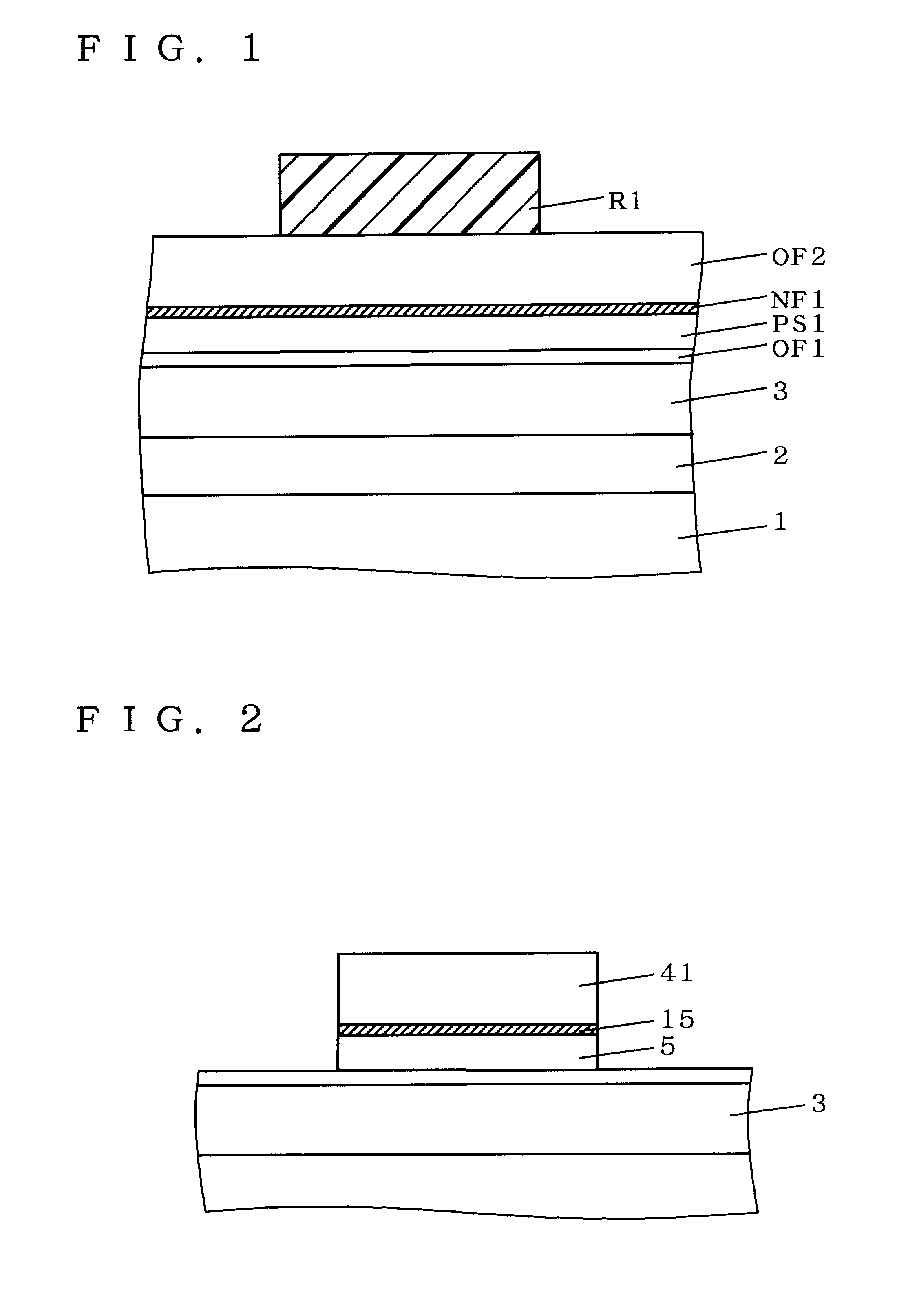
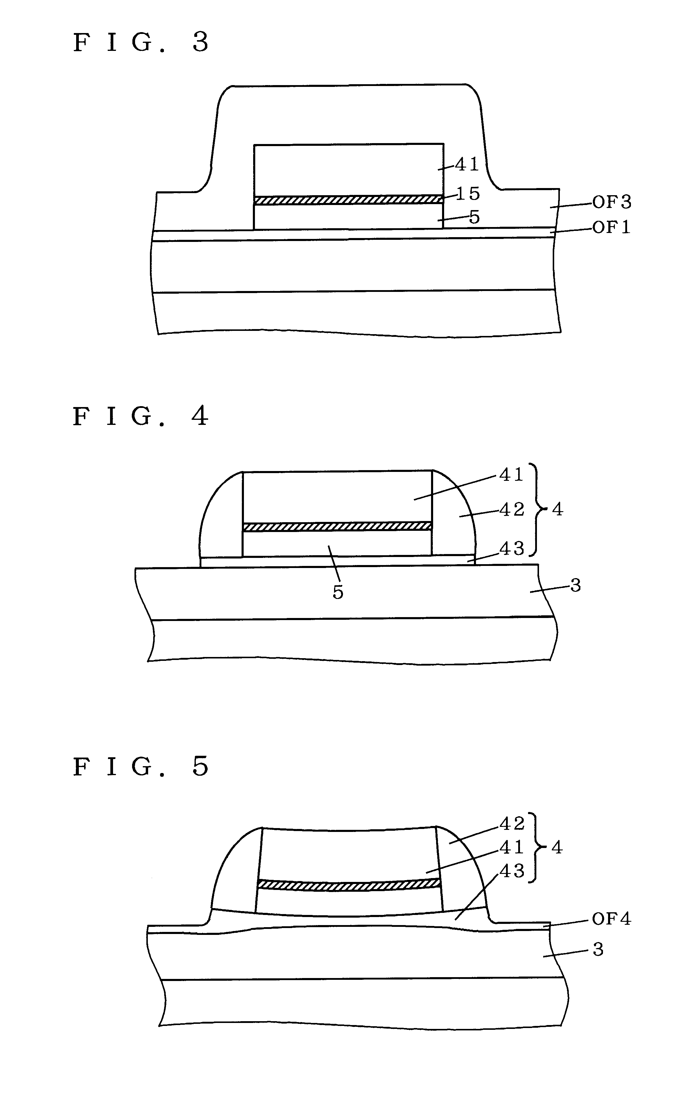
In the first to sixth preferred embodiments, semiconductor devices with field-shield isolation structure formed on the SOI substrate are discussed. It is natural that use of a bulk silicon substrate, instead of the SOI substrate, produces the same action and effect.

The seventh preferred embodiment discussed below produces marked action and effect when it applies to a semiconductor device with field-shield isolation structure formed on the SOI substrate.

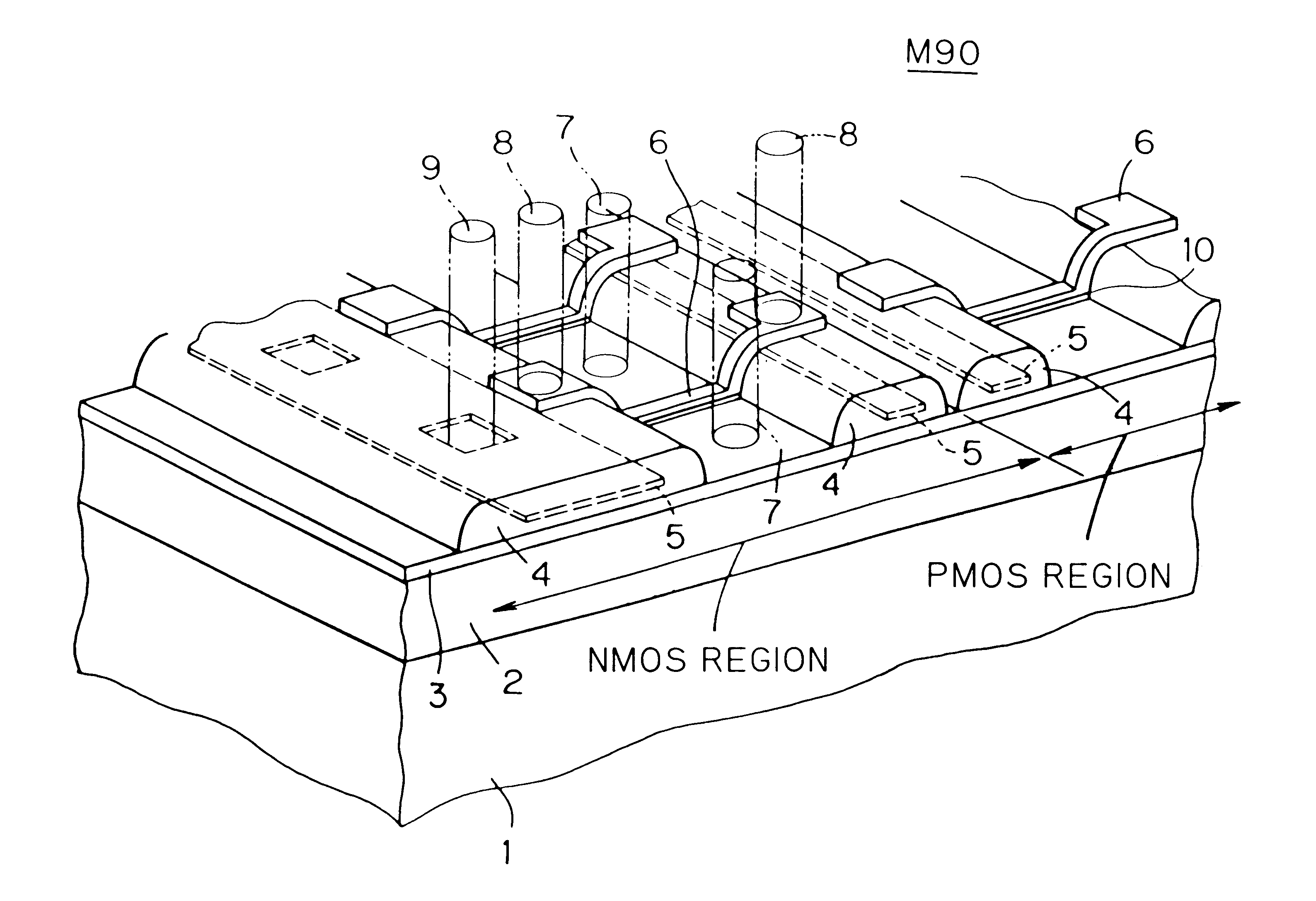
Since the SOI device has a structure where the channel is in a floating state, there is a problem of deterioration of drain breakdown voltage, for example, due to floating-substrate effect (an phenomenon caused by a channel in a floating state). To solve this problem, it is effective to fix the substrate potential, i.e., the channel potential by providing a body contact electrode. The semiconductor device with field-shield isolation structure is most suitable for providing the body contact electrode.

FIG. 58 is a plan vie...


PUM


Abstract

An FS upper nitride film (15) is formed on the upper surface of an FS electrode (5). Therefore, the upper surface of the FS electrode (5) is not exposed even when an FS upper oxide film (41) is partially almost removed in the manufacturing process. Thus, a semiconductor device which prevents degradation in operation characteristics and reliability due to existence of an FS insulating layer can be provided.

Description

1. Field of the InventionThe present invention relates to a semiconductor device and a manufacturing method therefor, and more particularly to a semiconductor device with field-shield isolation structure and a manufacturing method therefor.2. Description of the Background ArtFIG. 82 is a sectional perspective view of a semiconductor device M90 with field-shield isolation structure in the background art of the present invention. This is an SOI (Semiconductor-On-Isolation) type semiconductor device using an SOI substrate which has a film-like semiconductor layer, i.e., an SOI layer on an insulating substrate as a semiconductor substrate in which a transistor element is provided.In the semiconductor device M90, as shown in FIG. 82, a silicon semiconductor layer is formed as an SOI layer 3 on an insulating substrate constituted of a supporting substrate 1 and a buried oxide film 2. The SOI layer 3 includes a region where each of many NMOS transistors is formed (referred to as "NMOS regi...

Claims


Application Information

Patent Timeline
Patent Type & Authority Patents(United States)
IPC IPC(8): H01L21/765H01L21/70H01L21/76H01L29/786
CPCH01L21/765H01L21/76
Inventor MAEDA, SHIGENOBUIWAMATSU, TOSHIAKIMAEGAWA, SHIGETOIPPOSHI, TAKASHIYAMAGUCHI, YASUOHIRANO, YUICHI
Owner MITSUBISHI ELECTRIC CORP
Why Eureka
Try Eureka